Open Nav


The global Electronics Supply Chain has shifted dramatically toward China over the past two decades, and nowhere is that concentration more evident than in High-density Interconnect (HDI) Pcb Manufacturing and Smt Assembly. Chinese fabs now produce the majority of the world's HDI boards — from smartphone coreboards and wearable modules to automotive ADAS processors and medical imaging equipment. Understanding what Chinese HDI manufacturers actually offer, and where the real engineering challenges lie, is essential for anyone sourcing advanced assemblies in 2026.
HDI technology is not a single product category; it is a set of Manufacturing capabilities that push Pcb density far beyond what conventional multilayer boards can achieve. Microvias, sequential lamination, any-layer interconnection, and ultra-fine trace geometries all fall under the HDI umbrella. Each capability introduces tradeoffs between cost, reliability, and design flexibility. This article breaks down the core HDI technologies relevant to Smt Assembly, explains how Chinese manufacturers have scaled those capabilities to high volume, and identifies the design and sourcing decisions that separate a successful HDI project from a costly failure.
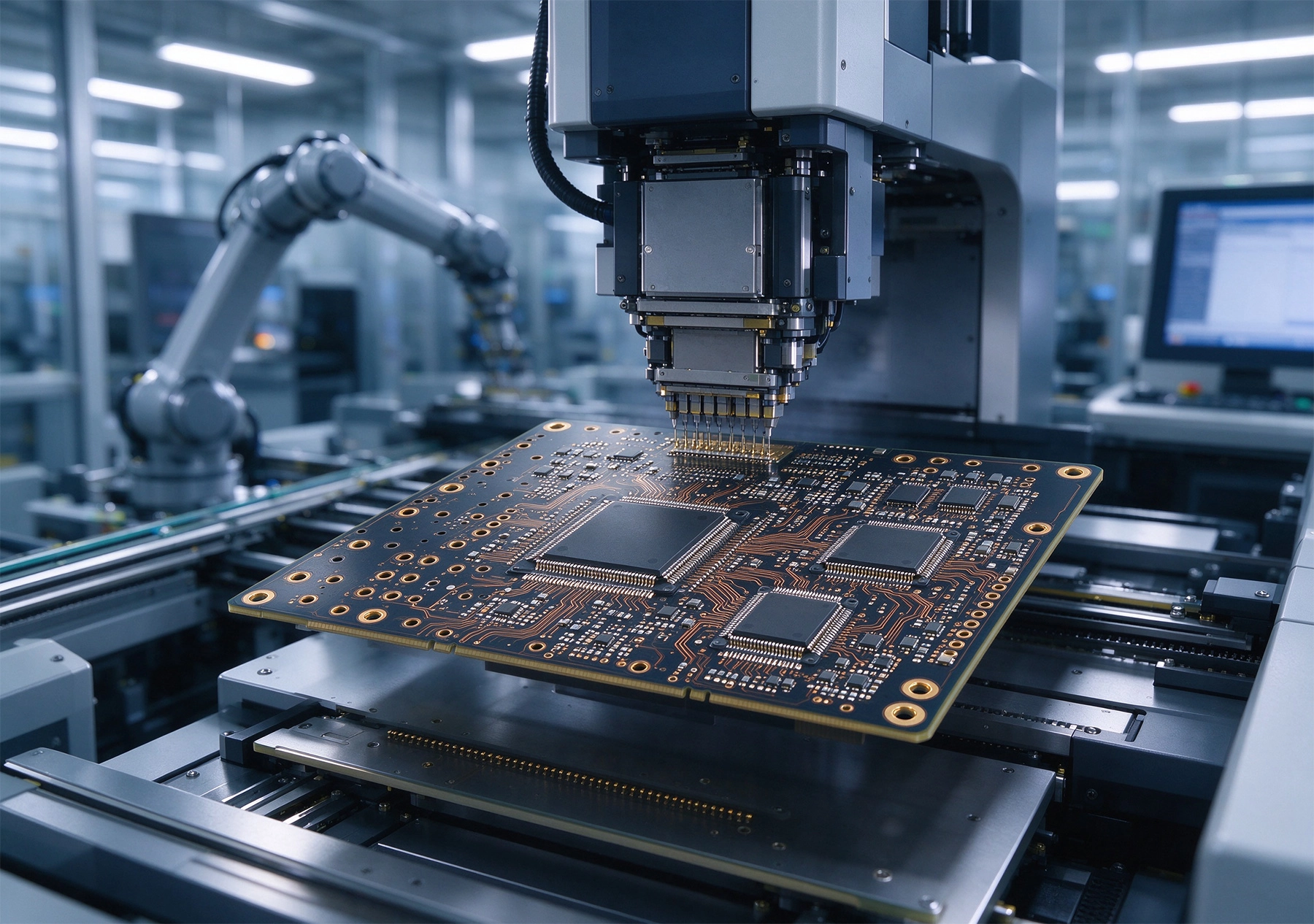
A conventional multilayer Pcb routes signals on outer layers and connects them through plated through-holes that run the full board thickness. An HDI board adds one or more layers of microvias — laser-drilled blind vias that connect only adjacent layers — allowing signals to escape from the interior of a dense Bga Package without consuming routing space on every layer. The result is a dramatic increase in routing density, a reduction in layer count for equivalent connectivity, and shorter signal paths that improve electrical performance.
For SMT assembly, HDI matters because it enables the use of fine-pitch Bga and CSP (Chip Scale Package) components that would simply be unmountable on a conventional board. A 0.35 mm pitch Bga with eight rows of balls requires over 200 routing connections. On a non-HDI board, those signals need to fan out across multiple layers with large annular rings and clearance holes — consuming significant board area and adding inductance. On an HDI board, the inner-row signals can escape through microvias placed directly under the outer balls, dramatically reducing the routing burden and the overall package footprint.
China's HDI Manufacturing base developed rapidly to serve the smartphone industry, which is one of the most demanding customers in electronics. The combination of extreme volume, aggressive cost pressure, and relentless miniaturization forced Chinese fabs to invest heavily in laser drilling, sequential lamination, and fine-line patterning capabilities that now serve a much broader range of applications.
Microvias are the defining feature of HDI boards. Unlike mechanically drilled through-holes, which are typically 0.3 mm or larger in diameter, microvias are laser-drilled with diameters ranging from 0.05 mm to 0.15 mm. The smaller diameter allows them to fit inside component pads, under BGA balls, and in routing channels where a standard through-hole would be impossibly large.
There are three common microvia types:
Staggered microvias appear on adjacent layers but do not overlap directly. Each via connects one layer to the next, and signals route through a stack of staggered microvias to travel between non-adjacent layers. Staggered microvia stacks are simpler to manufacture and are the standard entry point for HDI capability.
Stacked microvias align vertically — a via on layer 1–2 sits directly on top of a via on layer 2–3. This allows a direct vertical connection across multiple layers without consuming routing space on intermediate layers. Stacked microvias require more precise sequential lamination and are more sensitive to Thermal Stress because the stacked geometry concentrates mechanical load at the via interface. They are common in smartphone coreboards where routing density is paramount.
Consecutive blind vias connect multiple layers in a single drilling pass — for example, a laser drill that penetrates through the build-up layers to reach an internal plane without going further. These are used in specific stackup configurations where the build-up sequence creates the via geometry naturally. They are less common than staggered or stacked microvias but appear in certain high-density routing scenarios.
From a manufacturing standpoint, laser drilling is the critical process step. Carbon dioxide (CO2) lasers are used for larger microvia diameters (typically above 0.1 mm), while UV lasers handle the smaller sizes needed for ultra-fine-pitch components. Some advanced fabs use a combination of both in a single machine to optimize for the full range of via sizes on a complex board. The quality of the desmear process — removing the resin smear left inside the microvia after drilling — is as important as the drilling itself, because any residual resin insulates the barrel from the copper plating and creates an open circuit.
HDI boards achieve their density through a build-up process: alternating layers of dielectric (prepreg or resin-coated dielectric) and copper are laminated sequentially, with microvias drilled and plated after each lamination cycle. This sequential build-up allows the designer to place routing and plane layers anywhere in the stackup and connect them with microvias as needed.
The most common HDI stackup configurations are named after their via structure:
1-N-1 is the simplest HDI structure: one layer of microvia on each side of a core. This adds microvia capability to a conventional multilayer board and is widely available from most Chinese fabs that offer HDI service. It is the most cost-effective HDI entry point and handles most fine-pitch BGA applications up to around 0.4 mm pitch.
2-N-2 adds two layers of microvia on each side of the core, enabling higher routing density and any-layer interconnection within the build-up section. 2-N-2 is the standard configuration for smartphone main boards and is widely used in tablets, high-end wearables, and Automotive Electronics modules.
3-N-3 and higher configurations are used in the most advanced applications — silicon interposer substrates, high-performance computing modules, and specialized military and aerospace electronics. These are niche products manufactured by a small number of specialized fabs and carry significantly higher cost and lead time.
Each additional HDI layer requires another lamination, drilling, and plating cycle, which adds cost and extends the process timeline. Chinese manufacturers have optimized the 1-N-1 and 2-N-2 processes for high volume, making them cost-competitive with conventional multilayer boards for equivalent complexity. The key insight for designers is that a 2-N-2 board with six routing layers can often achieve the connectivity of an eight or ten-layer conventional board at a lower total cost and smaller footprint — but only if the design is actually HDI-optimized rather than a conventional design loosely mapped onto an HDI stackup.
Any-layer interconnection — sometimes called any-layer HDI (ALH) or simply "any layer" — means that any pad on any internal layer can be connected to any other pad on any other layer through a combination of microvia and routing paths. This is the capability that enables the extreme miniaturization of modern smartphones: the entire processor, memory, and power management subsystem can be routed in a stackup thinner than 1 mm.
Achieving any-layer interconnection requires precise control of the sequential lamination process. Each layer must be manufactured to tight tolerances for registration, dielectric thickness, and copper distribution, because errors accumulate across the lamination sequence. The fab must also maintain strict process controls for laser drilling, desmear, and plating across every cycle. Any contamination or process drift compounds across subsequent layers, which is why any-layer HDI is considered a high-end capability even among manufacturers that offer standard HDI services.
Not all Chinese fabs offering "HDI" service are capable of true any-layer interconnection. Buyers should verify the specific process capability — a fab may have 1-N-1 or 2-N-2 capability but not the precision controls needed for any-layer. Asking for a capability data sheet, a cross-section sample, or a DFM report from a similar build is the standard way to confirm this before committing to production.
The SMT assembly of fine-pitch components on HDI boards introduces its own set of challenges, separate from the board fabrication itself. Components with ball pitches of 0.4 mm and finer — increasingly common in application processors, RF transceivers, and power management ICs — demand a combination of fine-pitch Stencil Design, precise paste printing, and accurate placement that stretches the limits of standard SMT equipment.
Stencil Design for 0.4 mm pitch BGAs typically uses laser-cut apertures with polished walls to promote clean paste release. The stencil thickness is a balance: thick enough to deposit sufficient solder volume for reliable joint formation, thin enough to avoid bridging between adjacent pads. Common stencil thicknesses range from 0.08 mm to 0.12 mm for 0.4 mm pitch applications, with aperture designs that account for the component manufacturer's recommended paste volume.
Modern SMT lines use 3D SPI (Solder Paste Inspection) after printing to catch insufficient paste, bridging, or misalignment before the component is placed. For high-mix low-volume HDI assemblies — common in Industrial Electronics and medical devices — the SPI data provides a quality record that helps identify systematic process issues before they generate field failures.
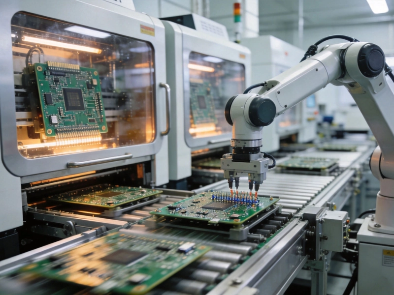
Placement accuracy for fine-pitch components requires vision systems that can identify the component package and correct for any misalignment in real time. Advanced pick-and-place machines achieve placement accuracy of ±0.025 mm at 3σ, which is sufficient for 0.4 mm pitch components when combined with self-centering paste forces during reflow. For 0.3 mm pitch and finer, some manufacturers add post-placement inspection with X-ray or acoustic microscopy to verify solder joint integrity before reflow — an added step that increases cost but catches defects that would otherwise surface only during ICT or functional test.
China's HDI manufacturing base is not monolithic. It spans a wide range of capability levels, from small shops running single lamination cycles on simple two-layer HDI boards to large-scale manufacturers with fully automated sequential build-up lines producing millions of units per month for major smartphone brands.
The high-volume consumer electronics segment — smartphone mainboards, tablet coreboards, smartwatch modules — is dominated by a handful of large Chinese manufacturers who have invested heavily in automation, process control, and yield optimization. These fabs operate at costs that are difficult to match elsewhere, largely because of scale, vertical integration (many run their own laminate prepregging and plating operations), and a deep Supply Chain of specialized materials and equipment within China.
The industrial and medical segment is served by a different tier: mid-sized manufacturers with strong DFM engineering support, flexible batch sizes, and the ability to handle more complex stackups without the volume minimums required by the largest consumer-focused fabs. These shops are the right choice for HDI boards in industrial controls, medical devices, Automotive Electronics modules, and aerospace applications where reliability traceability, documentation, and engineering collaboration matter as much as unit cost.
For buyers sourcing HDI assemblies in China, the key is matching the supplier tier to the application. A smartphone board fab may offer rock-bottom pricing but be unwilling to accept a 500-unit order with custom stackup requirements and detailed quality documentation. Conversely, a small boutique fab that handles high-reliability aerospace boards may quote prices that make no sense for a 50,000-unit consumer product. Understanding which tier you are dealing with before entering negotiations saves time and prevents frustration.
Designing for Hdi Assembly is not the same as designing a conventional multilayer board. The constraints are different, and ignoring them produces designs that are either unmanufacturable or require significant cost premiums to produce.
Trace and space geometries on HDI boards can be significantly finer than on conventional boards — 50 μm trace and space is standard at many Chinese fabs, with advanced shops offering 30 μm or below. However, fine traces require tighter impedance and DFM control, which means the fab must run tighter process tolerances. The cost difference between 75 μm and 50 μm trace and space is not huge in absolute terms, but the yield impact and the test coverage requirements make the finer geometry more appropriate for high-value boards where the cost of the board is a small fraction of the total product value.
Pad Design for microvia-in-pad (VIP) is a common requirement on HDI boards, particularly under BGAs. The microvia inside the pad must be filled and planarized before the component lands on it, which adds process steps and cost. Some designs can avoid VIP by using dog-bone fanout patterns — routing the signal from the BGA pad to a nearby microvia rather than placing the via inside the pad — at the cost of additional routing channel consumption. The choice between VIP and dog-bone fanout is a trade-off between routing density and manufacturing cost that should be resolved during the Dfm Review stage.
Thermal Management on HDI boards requires more attention than on conventional boards, because the multiple thin dielectric layers have lower thermal conductivity than a solid core. Thermal vias under power components, and careful attention to the thermal path through the stackup to the mounting heatsink interface, are essential for boards that dissipate significant power. The laser drilling process creates microvias that are actually beneficial for thermal spreading, because the copper-plated barrel of a thermal microvia conducts heat through the thin dielectric more effectively than the dielectric itself.
HDI boards for SMT assembly are evaluated against the same Ipc Standards as conventional boards, with specific addenda for HDI structures. IPC-2226 defines the design standard for HDI printed boards, covering microvia geometry, stackup requirements, and Dfm Guidelines. IPC-6016 is the qualification and performance specification for HDI boards, defining the test methods and Acceptance Criteria for microvia reliability, dielectric integrity, and thermal cycling performance.
For high-reliability applications — automotive under-hood electronics, medical devices, industrial controls — the IPC Class 3 requirements apply, with additional internal specifications from the OEM often layered on top. These requirements cover thermal cycling to defined temperature ranges, thermal shock, ionic contamination limits, and dielectric withstanding voltage. HDI microvia reliability under thermal cycling is a well-characterized failure mode, and the IPC-6016 test sequences are specifically designed to expose microvia fatigue failures that would not appear in standard electrical continuity testing.
X-ray inspection is standard for HDI assemblies with BGA and CSP components, because the joints are hidden beneath the component body. Automated X-ray inspection (AXI) systems can detect opens, voids, bridging, and insufficient solder volume without decapsulating the component. For boards with ultra-fine-pitch components, acoustic microscopy (SAT or C-SAM) provides additional sensitivity for delamination and interfacial voids that X-ray may not detect.
China's HDI manufacturing capabilities have matured to the point where they serve as the primary supply source for some of the most advanced electronics in the world. The combination of Microvia Technology, sequential lamination, fine-line patterning, and high-volume SMT assembly in a single region creates significant advantages in cost, Supply Chain efficiency, and engineering collaboration for teams that know how to navigate it.
The engineering challenges of HDI are real but manageable. Understanding microvia types, stackup configurations, and the specific process capabilities of your chosen fab — and designing accordingly — is the foundation of a successful HDI project. Working with a manufacturer that provides genuine DFM feedback rather than simply building to your files is the single most effective way to avoid the yield surprises and reliability failures that can turn a cost-saving initiative into a warranty nightmare.
Contact us to discuss your requirements.

Simplifying NPI (New Product Introduction) with Turnkey ManufacturingSeptember/01/2026
Custom Box Build Assembly: Integrating Mechanics and Electronics SeamlesslySeptember/03/2026
Handling 01005 Components and Micro BGAsJune/03/2026
Managing Moisture Sensitivity Levels (MSL) for BGA and QFN PackagesAugust/10/2026
Accelerating Time-to-Market with One-Stop PCB Assembly SolutionsJuly/07/2026
Why High-Reliability PCB Assembly is Critical for Medical DevicesMay/22/2026
Solving Assembly Stress Issues in Large and Thin PCBsSeptember/09/2026

Meet the Team: Expertise Behind Our High-Yield Production LinesSeptember/02/2026