If you have ever stood on a
Manufacturing floor staring at a tray of rejected boards, you know the frustration. Fixing Common SMT Defects: A Root Cause Analysis Approach is something every process engineer has to master eventually. You can't just keep reworking boards or tweaking machine settings blindly; that is a recipe for burning cash and missing shipment deadlines. Instead of treating the symptoms, we need to dig into the actual source of the problem.
I remember a time when our line suddenly started producing a massive amount of solder bridges on a new product. The team was convinced it was a bad batch of
Solder Paste. We switched pastes three times before someone finally checked the stencil
Aperture Design against the updated
Pcb layout. Turns out, the board designer had shrunk the pad spacing, but nobody updated the stencil file. In this article, I'll walk you through a systematic way to tackle these issues using real-world examples so you can stop guessing and start fixing.
 The 63% Rule: Start at the Stencil Printer
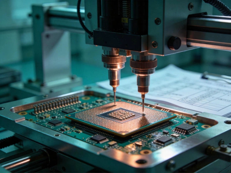
When you are Fixing Common SMT Defects: A Root Cause Analysis Approach, industry data tells us where to look first. Studies consistently show that about 63.8% of all SMT defects originate from the
Solder Paste Printing process. If your paste volume is wrong, no amount of tuning on the pick-and-place machine will save you.
Let’s talk about insufficient solder or dry joints. Usually, this means the apertures are clogged, or the squeegee pressure is too low. But sometimes, it's a simple issue like the paste being left out of the fridge for too long, causing the flux to evaporate and the paste to stiffen. Always check your printing parameters first. Are you using auto-underwipe correctly? Is the blade angle right? Get a 3D SPI (
Solder Paste Inspection) machine involved early to measure actual volume before the components even get placed.
Tombstoning: The Tug-of-War Effect
Tombstoning is one of the most annoying issues when Fixing Common SMT Defects: A Root Cause Analysis Approach. It happens when one end of a chip component lifts up during reflow, looking like an Egyptian monument. The root cause is almost always uneven surface tension. Basically, one side melts faster than the other, pulling the component upright.
To fix this, you need to look at thermal distribution. Is there a heavy copper plane connected to only one pad? That pad acts as a heat sink and delays melting. You can fix this by adding thermal relief pads or adjusting the pad geometry to be perfectly symmetrical. Also, check your reflow profile. If the preheat zone is too steep, the temperature gradient across the tiny component will trigger the imbalance. Slowing down the ramp-up rate often gives the whole board time to equalize thermally.
Solder Bridging and Shorts
Bridging occurs when solder connects two adjacent pads that shouldn't touch. When Fixing Common SMT Defects: A Root Cause Analysis Approach for shorts, don't just blame the printer. While excess paste is a common culprit, placement accuracy matters just as much. If the pick-and-place machine drops a QFN package slightly off-center, the excess solder on one side will flow over to the next pin during reflow.
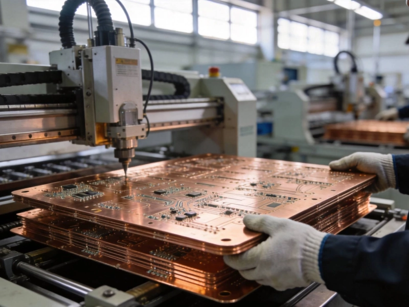
Another hidden cause is poor wetting due to oxidized pads or old paste. If the solder doesn't want to stick to the copper pad, it will ball up and bridge between pins instead. Make sure your
Pcb vendor is storing bare boards properly, and always verify your paste expiration dates. For fine-pitch components, reducing the stencil thickness from 5 mils to 4 mils can physically limit the amount of solder deposited, acting as a mechanical safeguard against bridges.
Voids and Cold Joints
Voids are trapped gas bubbles inside the solder joint. When Fixing Common SMT Defects: A Root Cause Analysis Approach for voiding, especially under large BGAs or QFNs, you have to manage outgassing. The flux inside the paste needs to escape before the solder turns completely liquid. If the ramp rate is too fast, the flux boils violently and gets trapped.
Cold joints look dull and grainy, usually caused by movement while the solder is solidifying, or inadequate heat. Check your conveyor speed and peak temperature. If the board isn't reaching liquidus long enough, the intermetallic layer won't form properly. I've also seen cold joints caused by excessive nitrogen flow in the oven blowing the heat away from the board. Balance your atmosphere settings carefully.
Conclusion: Data Over Guesswork
Fixing Common SMT Defects: A Root Cause Analysis Approach requires discipline. Stop making assumptions based on what worked last time. Every board design, every component package, and every environmental change requires a fresh look. Document your findings, use cross-sectioning when necessary, and trust your inspection data.
By focusing on the root causes—whether it's
Stencil Design, thermal profiles, or material handling—you will drastically reduce your defect rates. Take these strategies back to your production line today, and watch your first-pass yield climb.
Frequently Asked Questions
Q: What is the most common SMT defect?
A: Insufficient solder and
Solder Bridging are typically the top two, both heavily tied to the printing process.
Q: How do I prevent tombstoning?
A: Ensure symmetrical
Pad Design, avoid connecting pads directly to large copper pours without thermal relief, and optimize your preheat ramp rate.
Q: Can bad PCB fabrication cause SMT defects?
A: Absolutely. Warped boards, oxidized pads, or incorrect hole sizes can ruin even a perfectly tuned SMT line. Always inspect incoming bare boards.