Open Nav


The artificial intelligence revolution has fundamentally transformed computing infrastructure, creating unprecedented demand for specialized hardware capable of processing massive workloads. At the heart of this transformation lie AI servers—purpose-built systems optimized for Machine Learning training, inference, and high-performance computing. These servers rely heavily on advanced high-density interconnect (HDI) Pcb technology to achieve the computational density, signal integrity, and thermal performance required by modern AI applications. As AI continues to expand from research laboratories into enterprise data centers, edge computing environments, and consumer devices, the impact on HDI pcb assembly has been profound, driving technological innovations and reshaping Manufacturing priorities across the electronics industry.

Understanding the impact on HDI pcb assembly requires context on the scale and characteristics of AI infrastructure deployment. The growth trajectory has been nothing short of extraordinary, with implications extending far beyond traditional computing markets.
The AI server market has experienced exponential growth over the past decade, driven by breakthroughs in deep learning, increasing enterprise adoption, and the proliferation of AI across industries. Market projections suggest sustained compound annual growth rates exceeding 30% through the remainder of this decade, far outpacing traditional server markets.
This growth stems from diverse application areas. Large language models and generative AI require massive training clusters involving thousands of GPUs. Recommendation systems and real-time analytics demand inference capabilities deployed across distributed infrastructure. Edge AI applications in automotive, industrial automation, and smart cities create new deployment scenarios with unique requirements.
AI workloads differ fundamentally from traditional computing in their computational requirements. Training modern neural networks can require tens of petaflops of computing power sustained over extended periods. Even inference workloads, which once ran on modest hardware, now demand substantial parallel processing capability as models grow in size and complexity.
This computational density translates directly into hardware requirements. AI servers typically incorporate multiple high-performance GPUs or specialized accelerators arranged in tight configurations. Each accelerator may contain thousands of processing cores and hundreds of gigabytes of high-bandwidth memory. The interconnects between these components must operate at unprecedented speeds while maintaining signal integrity across complex routing structures.
The computational power of AI servers comes with substantial energy requirements. A single high-end AI server can consume 10-20 kilowatts of power under full load, compared to 1-3 kilowatts for traditional servers. This power consumption generates enormous heat that must be removed efficiently to prevent performance degradation or component failure.
Thermal Management is particularly challenging because heat sources are distributed throughout the system rather than concentrated in a small area. Multiple processors, memory modules, power regulators, and interconnect switches all generate significant heat that must be managed simultaneously without creating thermal gradients that affect reliability.
Enterprise AI deployments, particularly those supporting mission-critical applications, demand exceptional reliability. Training runs can last weeks or months, with failures costing millions in lost computation time. Inference systems must maintain high availability to support real-time applications where downtime is unacceptable.
These requirements extend to the underlying Pcb technology. Boards must maintain signal integrity and thermal performance over extended periods under demanding conditions. Component aging, thermal cycling, and electrical stress must not compromise the reliability needed for continuous operation.
The demands of AI servers have accelerated the adoption and evolution of HDI PCB technology. Understanding these fundamentals is essential for appreciating the Manufacturing challenges and innovations driven by AI requirements.
HDI technology relies on microvias—small laser-drilled holes typically 50-150 micrometers in diameter—to create electrical connections between layers without consuming the large area required by traditional through-hole vias. AI server boards routinely use microvias densely packed throughout the board to enable the routing density needed for complex processor and memory interconnects.
Sequential lamination processes build boards layer by layer, enabling microvias to be placed on inner layers and stacked to create connections between non-adjacent layers. AI server designs often employ 10-20 layer stacks with microvias on every layer, creating three-dimensional interconnect structures that would be impossible with conventional PCB technology.
Component pin counts in AI accelerators and high-speed memory interfaces continue to increase, requiring ever-finer trace widths and spaces. Modern AI server boards routinely use traces as small as 2-3 mils (0.05-0.075 mm) with matching spacing, enabling component pitches that would be impossible with standard PCB technology.
These fine traces present manufacturing challenges including etching precision, impedance control, and defect detection. Advanced photolithography and controlled etching processes are essential to achieve consistent results across large board areas with high trace density.
Blind and buried vias enable interconnects that don't span the entire board thickness, freeing up routing space on layers not involved in the connection. AI server designs leverage these capabilities extensively to route thousands of signals between processors, memory, and interconnects while maintaining signal integrity and minimizing crosstalk.
The prevalence of blind and buried vias in AI designs necessitates advanced inspection capabilities. X-ray inspection systems must detect plating voids and alignment issues in buried structures that are invisible to optical inspection.
AI server boards operate at signal frequencies that would have been unimaginable a decade ago. Interconnects between processors and memory routinely operate at 28-56 gigabits per second, with even faster speeds on the horizon. These speeds demand PCB materials with exceptional electrical characteristics.
Low dielectric loss materials minimize signal attenuation at high frequencies. Stable dielectric constants ensure predictable impedance control. Low moisture absorption maintains electrical characteristics in varying environmental conditions. These material requirements drive adoption of specialized high-frequency materials that differ substantially from standard FR-4.
The unique requirements of AI server hardware have created specific challenges in HDI Pcb Assembly that differ from traditional high-volume consumer electronics or standard server applications.
AI servers incorporate some of the most complex integrated circuits ever manufactured. Large array Bga packages with thousands of pins, footprint sizes exceeding 50mm square, and fine pitch requirements below 0.8mm are standard. These components present assembly challenges at every stage.
Stencil Design must achieve consistent paste deposition across large areas while avoiding bridging on fine-pitch pins. Reflow profiles must accommodate the thermal mass of large packages while preventing thermal damage to adjacent components. Inspection systems must detect defects in dense solder joint arrays where optical access is limited.
Assembly yields on these components are often the limiting factor in overall system cost. Even small defect rates can result in expensive rework or scrap due to the high component cost and limited repair options on complex packages.
Assembly processes must accommodate sophisticated Thermal Management solutions. Heavy copper power planes, thermal vias arrays, and embedded metal cores must be integrated without compromising electrical performance or manufacturability. Thermal interface materials must be applied precisely to ensure optimal heat transfer between components and cooling solutions.
The assembly sequence must account for thermal management components that may be installed after main Pcb Assembly. This creates complex coordination between PCB assembly, mechanical assembly, and system integration processes.
AI servers require sophisticated power distribution networks to deliver clean, stable power to multiple processors and memory modules simultaneously. These networks involve multiple voltage rails, high-current switching regulators, and extensive filtering networks.
Assembly must ensure reliable connections to large power connectors and high-current components. Solder joint integrity becomes critical when carrying hundreds of amps of current. Component placement tolerances must accommodate mechanical stresses from large connectors and power distribution components.
High-speed interconnects are sensitive to assembly variations that can affect impedance and signal integrity. Controlled impedance traces require precise manufacturing control. Solder joint variations can introduce impedance discontinuities that degrade signal performance.
Assembly processes must minimize variations that affect signal characteristics while maintaining productivity. Process control extends beyond traditional dimensions to include electrical characteristics like impedance, crosstalk, and insertion loss.
The challenges posed by AI server hardware have stimulated innovation across the PCB assembly ecosystem. These innovations are pushing the boundaries of what's possible in high-volume manufacturing.
Traditional pick-and-place machines struggle with the component sizes and precision requirements of AI server boards. New generation equipment combines vision systems with sub-micron positioning accuracy, force-controlled placement to prevent damage to delicate components, and placement rates that maintain economic viability despite the complexity of AI boards.
Multiple head configurations enable simultaneous placement of different component types. Some systems incorporate specialized heads for large Bga packages that cannot be placed on standard equipment. Vision systems detect component lead coplanarity and other defects before placement, preventing costly defects.
Re soldering AI server boards requires precise control of thermal profiles. The large thermal mass of dense components and the presence of temperature-sensitive materials demand carefully engineered heating and cooling ramps. Modern reflow ovens use multiple heating zones with independent temperature control, real-time profile monitoring, and adaptive control to maintain optimal conditions.
Nitrogen atmosphere reflow reduces oxidation and improves joint quality, particularly important for high-reliability applications. Vacuum reflow technology eliminates voids in large area solder joints, critical for thermal performance and reliability under thermal cycling.
Traditional Automated Optical Inspection cannot adequately verify the dense, complex structures of AI server boards. Advanced systems incorporate multi-angle imaging, high-resolution cameras with sub-pixel precision, and sophisticated image analysis algorithms to detect subtle defects.
X-ray inspection has become essential for verifying solder joint quality in hidden locations, particularly under large BGAs and in stacked die packages. 3D X-ray tomography provides complete volumetric inspection of complex structures, detecting voids, insufficient solder, and bridging that would be invisible to surface inspection.
The cost and complexity of AI server boards make process monitoring essential. Real-time monitoring of stencil printing, component placement accuracy, and reflow profiles enables rapid detection and correction of process drifts before they produce defects.
Statistical process control systems track hundreds of process parameters, correlating variations with quality outcomes. Machine Learning algorithms analyze process data to identify subtle patterns that indicate developing problems before they affect product quality.
The rise of AI servers has created ripple effects throughout the Electronics Supply Chain, affecting everything from material selection to certification requirements.
The demand for specialized high-frequency PCB materials has created supply pressures and price increases. Low-loss dielectric materials, high TG laminates, and specialty prepregs have seen lead times extend and prices rise as manufacturers struggle to meet surging demand from AI and other high-performance applications.
Copper clad laminate manufacturers are expanding capacity and developing new materials optimized for AI applications. However, capital investment and material qualification processes mean that supply will lag demand for the foreseeable future.
PCB fabricators and assembly providers must invest in new equipment to meet AI server requirements. UV laser drilling systems, advanced plating lines, precision lamination presses, and sophisticated inspection equipment require significant capital investment.
This investment creates concentration in the manufacturing base, as only well-capitalized companies can afford the equipment needed for AI server boards. Smaller manufacturers either partner with larger facilities or focus on less demanding market segments.
The complexity of AI server boards demands skilled workers throughout the manufacturing process. Process engineers must understand high-speed electrical characteristics and their interaction with manufacturing processes. Quality technicians must interpret complex inspection data and make nuanced judgments about acceptable variations.
Developing this workforce requires ongoing training programs and partnerships with technical schools and universities. Companies that build internal expertise gain competitive advantages in this demanding market.
AI applications often operate in regulated environments requiring specific certifications. Automotive AI systems require automotive-grade qualification standards. Medical AI applications demand medical device compliance. Aerospace applications have military and aerospace specifications.
These certifications affect everything from material selection to process documentation. PCB manufacturers must maintain multiple certification programs and understand the specific requirements of each target industry.
AI server requirements are driving changes in design for manufacturability (DFM) practices. Designs that would have been considered unmanufacturable a few years ago are now routine, while new challenges emerge.
The complexity and cost of AI server boards mandate early collaboration between designers and manufacturers. Design reviews must include manufacturing representatives before final design approval. Prototyping strategies must account for the long lead times and high costs of specialized materials and processes.
Design-for-test considerations become increasingly important. Test access in dense designs requires strategic planning. Boundary Scan implementation, test point placement, and controllability/observability considerations must be integrated from the earliest design stages.
Thermal management must be co-designed with electrical performance, not treated as an afterthought. The choice between different thermal management approaches affects routing density, layer stack requirements, and material selection. Thermal simulations must inform electrical layout decisions.
This co-design extends to the system level. PCB thermal performance must be compatible with system-level cooling solutions. Mechanical constraints, airflow patterns, and heat sink attachment points must be integrated into Pcb Design.
Reliability requirements must drive design decisions rather than being addressed through design margins alone. Expected operational environments, mission profiles, and maintenance strategies must influence technology choices and design parameters.
Reliability Testing must be integrated into the development cycle. Accelerated life testing, thermal cycling tests, and vibration testing should inform design iterations rather than being reserved for final validation.
The evolution of AI technology continues, with implications for HDI PCB assembly that will shape the industry for years to come.
Advanced packaging approaches including chiplets and modular designs are changing how AI systems are constructed. Rather than single monolithic chips, systems are built from multiple specialized components interconnected via advanced packaging.
This trend affects Pcb Design and assembly in several ways. Interposer requirements become more sophisticated. Power distribution must accommodate multiple voltage domains. Testing complexity increases as systems become more modular but also more interconnected.
As AI moves to the edge—in vehicles, drones, industrial equipment, and consumer devices—form factor requirements become more stringent. These applications must deliver substantial AI capability in small, rugged, and often battery-powered packages.
This drives demand for even higher density HDI technology in smaller form factors. Ruggedization requirements add constraints on materials and assembly processes. Power efficiency becomes increasingly critical as battery life constraints dominate design decisions.
Emerging Ai Hardware approaches including neuromorphic computing and analog AI require different PCB characteristics than traditional digital designs. These architectures may emphasize different aspects of PCB performance such as analog precision or specialized interconnect architectures.
Assembly processes may need to accommodate different component types, different thermal characteristics, and different reliability considerations. The industry must develop expertise in these emerging architectures as they move from research to production.
Environmental concerns are increasingly influencing technology choices across all industries, including AI infrastructure. Energy efficiency improvements reduce both operating costs and environmental impact. Material choices increasingly consider lifecycle impacts and recyclability.
Assembly processes must adapt to reduce waste generation, improve energy efficiency, and minimize environmental footprints. These considerations may drive technology choices and process optimizations that have implications for cost and manufacturability.
The rise of AI servers has fundamentally reshaped HDI PCB assembly, driving technological innovation, creating new challenges, and reshaping industry dynamics. The computational density, signal integrity requirements, thermal management demands, and reliability needs of AI infrastructure have pushed PCB technology to its limits and stimulated breakthroughs across the assembly ecosystem.
This transformation is far from complete. As AI technology continues to evolve—through larger models, more sophisticated architectures, and expanding application areas—the demands on PCB assembly will continue to increase. Manufacturers that develop the capabilities to meet these challenges will find themselves at the forefront of one of the most important technology trends of our time.
The impact extends beyond AI-specific applications. Many of the technologies, processes, and capabilities developed for AI servers are finding applications in other high-performance computing areas, telecommunications infrastructure, and advanced automotive systems. The innovations driven by AI are raising standards across the entire electronics industry.
For PCB assembly providers, the rise of AI servers represents both a challenge and an opportunity. The technical requirements are demanding, the capital investments substantial, and the learning curves steep. However, the market growth is exceptional, the value proposition clear, and the strategic importance undeniable. Companies that successfully navigate this transition will be well-positioned for the technology-driven decades ahead.
Ultimately, the story of AI servers and HDI PCB assembly is a story of symbiotic evolution. AI drives PCB innovation, and PCB capabilities enable AI progress. This mutually reinforcing relationship will continue to shape both industries, pushing the boundaries of what's possible in electronic design and manufacturing.
AI server PCBs feature much higher component density, more complex layer structures, and more demanding signal integrity requirements. They typically use 10-20 layers with microvias on every layer, compared to 8-16 layers with fewer HDI features in traditional servers. Assembly requires more sophisticated equipment, tighter process control, and more extensive inspection capabilities.
The primary challenges include achieving consistent quality on large, complex BGAs with thousands of pins, maintaining impedance control on fine-pitch high-speed traces, managing thermal performance of high-power components, and detecting defects in dense, three-dimensional structures where optical access is limited. Yield management is also challenging given the high component costs.
AI server demand has strained capacity for advanced HDI manufacturing and specialized materials. Lead times for high-frequency materials and advanced PCB Fabrication have increased significantly. Manufacturers are investing in new equipment and expanding capacity, but the capital-intensive nature of these investments means that supply will lag demand for the foreseeable future.
Thermal management is critical because AI servers consume 10-20 kilowatts of power and generate substantial heat. Assembly must integrate thermal vias arrays, heavy copper planes, and thermal interface materials without compromising electrical performance. The assembly sequence must coordinate with thermal management components and system-level cooling solutions.
Yes, several emerging technologies are driven by AI requirements. Chiplet-based systems demand advanced interposer technology. Edge AI applications require even higher density HDI in smaller form factors. Neuromorphic computing may require different PCB characteristics than traditional digital designs. These trends will continue to drive innovation in materials, processes, and design approaches.
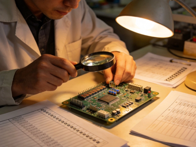
A Complete Checklist for Ordering Prototype PCB AssemblyOctober/10/2026
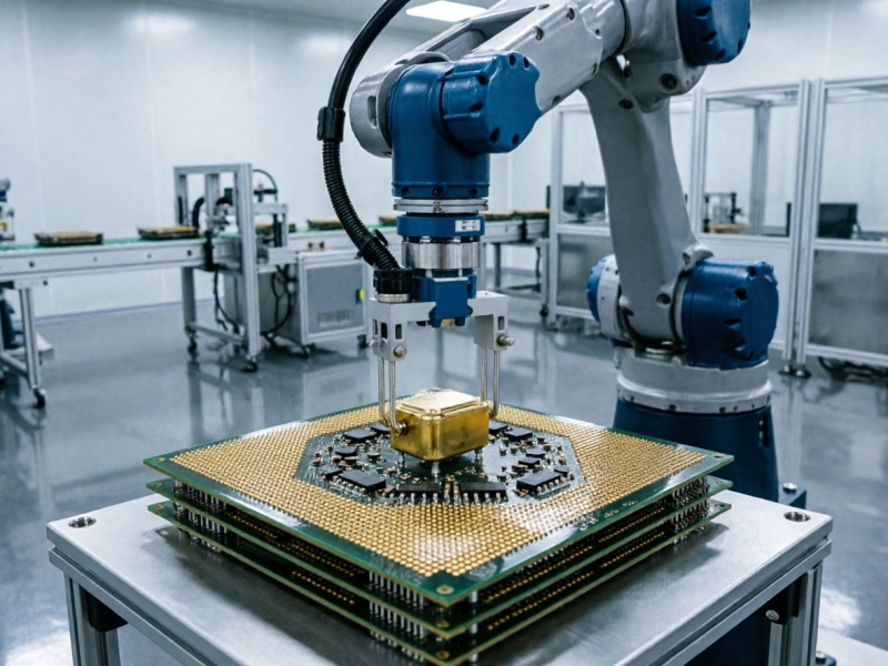
Understanding the True Cost Drivers in Modern Electronics ManufacturingJuly/20/2026
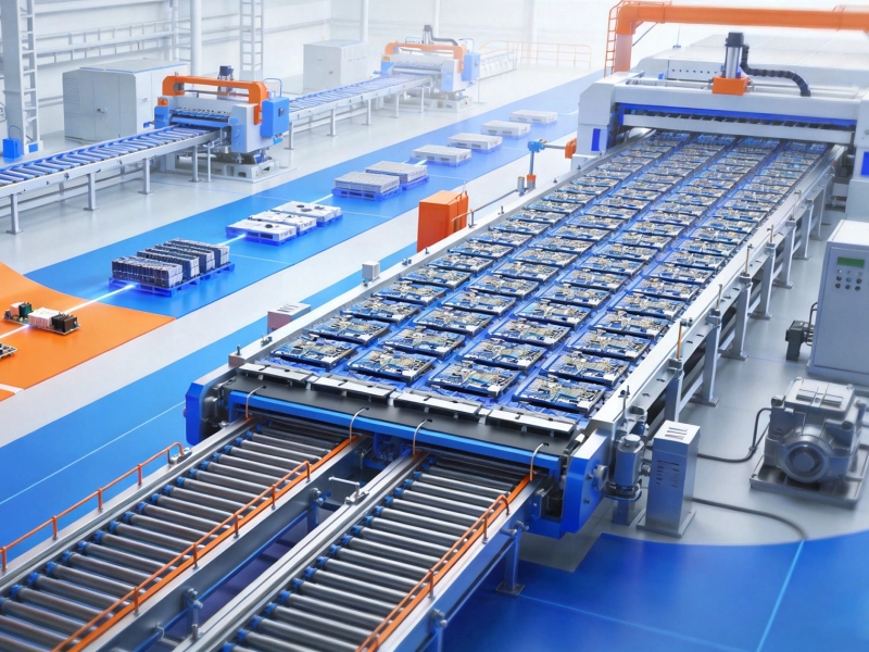
From Prototype to Mass Production: Scaling Your Hardware StartupSeptember/04/2026
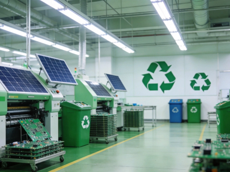
Sustainability in PCBA: The Push for Green and Lead-Free ProcessesJuly/28/2026

The State of Global PCBA Manufacturing in 2026 and Key TakeawaysMay/22/2026
Why High-Reliability PCB Assembly is Critical for Medical DevicesMay/22/2026
Why High-Reliability PCB Assembly is Critical for Medical DevicesJune/02/2026
How Automotive Electronics are Redefining PCBA Quality StandardsJuly/01/2026