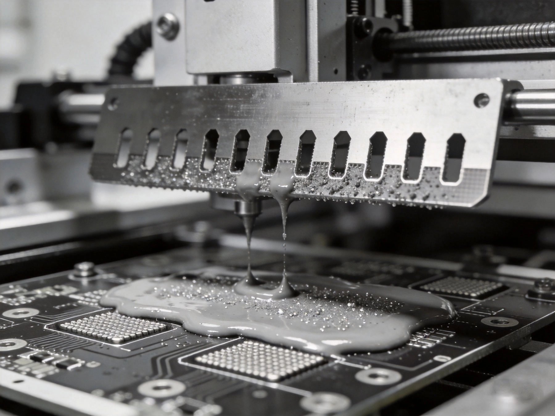
In the world of Surface Mount Technology (SMT) assembly, solder paste printing stands as the most critical—and often most problematic—process step. Studies consistently show that 50-70% of all SMT defects originate from poor solder paste printing. Yet despite its importance, stencil design is frequently treated as an afterthought rather than the precision engineering discipline it deserves to be.
The stencil isn't merely a piece of metal with holes cut in it. It's a precision tool that transfers exact quantities of solder paste to exact locations on your Pcb, enabling the formation of reliable solder joints that will determine your product's electrical performance and mechanical integrity for years of field operation. Getting it right requires understanding the science behind solder paste behavior, foil material properties, and aperture geometry optimization.

Understanding Solder Paste Behavior
Before diving into stencil design specifics, successful paste printing requires understanding how solder paste behaves during the application process:
The Composition Challenge
Solder paste is a heterogeneous mixture of:
- Metal particles: Typically SAC305 (96.5% Sn, 3% Ag, 0.5% Cu) or leaded alloys, with particle sizes ranging from Type 3 (25-45μm) to Type 5 (10-25μm)
- Flux: A chemical medium that cleans oxide layers, reduces surface tension, and protects the joint during reflow
- Vehicle: A binder system keeping particles suspended and providing desired rheological properties
The ratio of metal to flux (typically 85-90% metal by weight) directly impacts joint volume and solderability. This ratio must remain consistent through the printing process.
Rheological Properties
Solder paste exhibits complex flow behavior:
- Thixotropy: Shear-thinning behavior that allows paste to flow through apertures under print pressure but maintain shape when stationary
- Viscosity: Must be optimized for the specific aperture size and print parameters
- Tackiness: The ability to hold components in place after paste deposition, before reflow
- Slump resistance: Maintaining deposited shape without spreading between pads
Stencil Foil Materials: Making the Right Choice
Stainless Steel
The most common stencil material, available in various thicknesses:
- 300 series stainless: Excellent durability and corrosion resistance
- Typical thicknesses: 0.08mm (3mil) to 0.20mm (8mil)
- Best for: General-purpose applications with standard component pitches (0.4mm and above)
Carbon Steel
An economical alternative for high-volume production:
- Lower cost: Approximately 30-40% less expensive than stainless steel
- Higher stiffness: Better for very large stencils or certain squeegee configurations
- Best for: High-volume, cost-sensitive applications with established processes
Nickel
For the most demanding applications:
- Superior durability: 5-10x the life of stainless steel
- Fine feature capability: Excellent for ultra-fine pitch applications
- Electroforming process: Enables very smooth walls with precise dimensional control
- Best for: High-mix production with frequent changeovers, or ultra-Fine Pitch Components
Foil Thickness Selection
Stencil thickness directly impacts solder deposit volume. Key considerations:
- Aspect ratio: Aperture width divided by foil thickness; aim for >1.5 for reliable paste release
- Area ratio: Aperture area divided by aperture wall area; IPC-7525 recommends >0.66 for reliable printing
- Component requirements: Fine-pitch components need thinner stencils; large power components may need apertures that are partially blocked or stepped
- Typical thickness guidelines: 0.1mm for 0.4mm pitch, 0.12mm for 0.5mm pitch, 0.15mm for 0.65mm pitch and larger
Stencil Fabrication Methods
Laser Cutting
The dominant method for modern stencil production:
- Process: High-power laser vaporizes metal along the programmed path
- Advantages: Excellent dimensional accuracy, fast turnaround, cost-effective for most applications
- Wall quality: Slightly tapered walls (typically 2-5°) facilitate paste release
- Limitations: Minimum practical aperture size around 0.15mm; wall surfaces are not mirror-smooth
Chemical Etching
The traditional method, now largely superseded:
- Process: Photolithographic masking followed by chemical dissolution of unprotected metal
- Advantages: Very low cost, good for large apertures
- Disadvantages: Isotropic etching creates trapezoidal walls that hinder paste release; not recommended for fine-pitch work
Electroforming
For the highest precision applications:
- Process: Nickel is electrodeposited onto a mandrel with the inverse aperture pattern
- Advantages: Very smooth walls (mirror-like finish), excellent paste release, excellent durability
- Disadvantages: Higher cost, longer lead times, limited maximum size
- Best for: 0.3mm pitch and below, or applications requiring maximum yield improvement
Aperture Design Fundamentals
Basic Principles
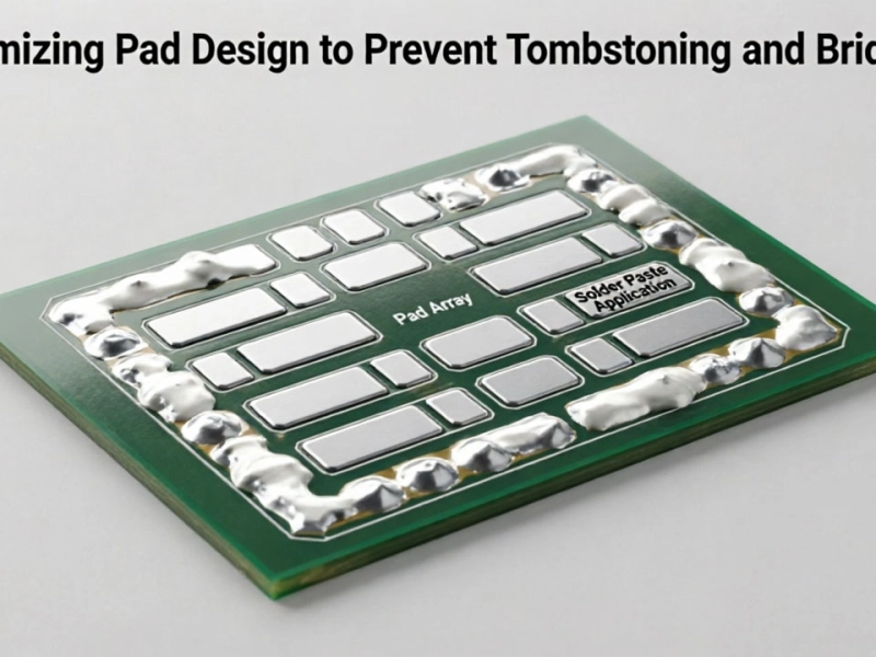
Aperture design directly determines solder joint quality. Key guidelines:
- Pad-to-aperture relationship: Standard practice is aperture size = pad size × 0.8 to 0.9 for most components
- Land area coverage: Typically 80-90% of the pad area for adequate solder volume
- Corner radius: Small radii (0.025-0.05mm) improve paste release compared to sharp corners
Component-Specific Aperture Strategies
Fine-Pitch Components (0.3mm - 0.5mm Pitch)
These demanding applications require careful optimization:
- Aperture reduction: 0.85-0.9× pad dimensions to prevent bridging
- Length extension: Slightly extend apertures in the print direction (1:1 to 1:1.2 ratio) for improved release
- Electropolished walls: Specify electropolishing for smoother walls and better release
- Smaller foil thickness: Use the thinnest foil that provides adequate volume
Fine-Pitch QFN/MLF Components
Bottom-terminated components present unique challenges:
- Thermal pad apertures: Often need custom aperture patterns to achieve uniform paste coverage across the entire pad
- Grid or array patterns: Multiple small apertures can improve paste spread compared to one large opening
- Step stencils: Lower step height over thermal pads to deposit more paste where needed
Large Components (Connectors, Transformers)
Components with thermal mass or multiple pads require adjusted strategies:
- Increased aperture ratio: 0.9-1.0× for adequate solder volume
- Corner clips removed: Avoid small apertures at pad corners that cause voiding
- Via-in-pad considerations: Plug or tent vias to prevent paste from wicking into holes
Advanced Stencil Techniques
Step Stencils
For assemblies with mixed component densities:
- Application: Some areas of the board require thicker paste deposits (BGA, QFN thermal pads) while others need standard deposits
- Construction: A step-up (thicker section) or step-down (thinner section) is chemically milled or added to specific board areas
- Design considerations: Step transitions must occur in non-critical areas; require careful squeegee technique
h3>Prototype Stencils
For rapid development, several options accelerate time-to-market:
- Framed stencils: Traditional design mounted in aluminum frames for use with standard printers
- Unframed stencils: Lower cost, requires alignment fixtures or manual printing
- NiGen electroformed prototypes: Premium option for complex prototype builds
nanotechnology Coatings
Advanced surface treatments improve paste release:
- Electropolishing: Creates smooth, mirror-like walls that facilitate paste release
- nanocoatings: Ultra-thin polymer layers that reduce surface energy and prevent paste sticking
- Material selection: Trudem鹰ite and similar proprietary coatings available for various foil materials
Print Process Optimization
Print Parameters
The stencil is only part of the equation. Successful printing requires optimized process parameters:
- Squeegee speed: Typically 20-80mm/s; slower speeds deposit more paste but reduce throughput
- Squeegee pressure: 4-8kg per 250mm of squeegee length; adjust to clean the stencil without flexing
- Squeegee material: Metal squeegees provide consistent pressure; rubber offers flexibility for uneven boards
- Snap-off distance: 0-2mm for most applications; larger for boards with height variation
- Print speed: Second print pass (where used) typically runs 50-70% of first pass speed
Board Support and Clamping
Proper board support prevents defects:
- Vacuum support: Essential for thin or flexible boards
- Magnetic pins: For boards with critical bottom-side clearances
- Clamping strategy: Prevents board movement without distorting panelized designs
- Panelization consideration: V-scored panels need edge support to prevent spreading during printing
Paste Handling and Storage
Paste condition directly impacts print performance:
- Refrigeration: Most pastes require 2-10°C storage to maintain rheological properties
- Acclimation: Allow paste to reach room temperature before opening containers (4-8 hours typical)
- Working life: Once opened, paste typically remains usable for 8-24 hours depending on conditions
- Reclaiming: Unused paste can often be returned to containers but should be monitored for contamination and flux separation
Quality Verification and Troubleshooting
Inspection Methods
Verifying paste deposition quality:
- 2D inspection: Area and coverage measurement; useful for trending but doesn't detect voids
- 3D inspection: Volumetric measurement providing excellent process control data
- Wet paste vs. post-reflow correlation: Understanding the relationship between paste volume and final joint quality
Common Defects and Solutions
Insufficient Paste Volume
- Increase aperture size by 5-10%
- Reduce squeegee speed
- Check foil thickness for accuracy
- Verify paste viscosity hasn't degraded
bridging / Excess Paste
- Reduce aperture size by 5-10%
- Increase squeegee speed
- Verify foil thickness isn't excessive
- Check for paste contamination or degradation
Poor Release / Smeared Paste
- Specify electropolished or coated stencil
- Increase snap-off distance
- Reduce squeegee pressure
- Check paste for separation or contamination
- Verify board flatness and support
Voiding in BGA Pads
- Consider aperture modifications (cross or slot patterns)
- Verify paste chemistry is suitable for BGA applications
- Evaluate stencil wall quality
- Review reflow profile for proper flux activation
Working with Your CM: Communication Best Practices
Information to Provide
When requesting stencils from your contract manufacturer:
- Gerber files: Include solder mask and paste layer Gerber files
- Bill of materials (BOM): Component list identifying special requirements
- Assembly drawings: Indicate any non-standard requirements or special components
- Board specifications: Material, thickness, surface finish, and any special requirements
- Quality requirements: IPC class if critical, any special inspection requirements
Questions to Ask Your Stencil Supplier
To ensure optimal results:
- What foil material and thickness do you recommend for my application?
- Will you apply any surface treatment to the stencil?
- What is your minimum aperture capability?
- Do you provide 3D paste inspection data with stencils?
- What is the lead time for my order quantity?
- Can you provide process optimization support if we experience defects?
Key Takeaways
- Solder paste printing is responsible for 50-70% of SMT defects; stencil design deserves serious engineering attention
- Foil material selection (stainless steel, carbon steel, nickel) impacts durability, cost, and print quality
- Stencil thickness and aperture geometry must be optimized for the specific component types and pitches
- Laser cutting provides the best balance of quality, turnaround, and cost for most applications
- Area ratio >0.66 and aspect ratio >1.5 are minimum targets for reliable paste release
- Step stencils address mixed-density assemblies with varied paste volume requirements
- Electropolishing and nanocoatings significantly improve release for challenging applications
- Print process parameters (speed, pressure, snap-off) must be optimized for each stencil-board combination
- 3D paste inspection provides critical data for continuous process improvement
- Close communication with your CM and stencil supplier ensures optimal results
Frequently Asked Questions
What is the typical lifespan of a laser-cut stainless steel stencil?
Laser-cut stainless steel stencils typically last 20,000-50,000 prints depending on foil thickness, print parameters, and board surface finish. Thinner stencils wear faster. Nickel electroformed stencils can last 100,000+ prints. Monitor paste transfer efficiency over time; when deposits become inconsistent, it's time for stencil replacement. Regular cleaning between print runs extends stencil life significantly.
How do I determine the optimal stencil thickness for my application?
Start with these guidelines: 0.08mm (3mil) for ultra-fine pitch (0.3mm and below), 0.10mm (4mil) for 0.4mm pitch, 0.12mm (5mil) for 0.5mm pitch, and 0.15mm (6mil) for 0.65mm pitch and larger. However, the optimal thickness also depends on aperture geometry—verify that your aperture designs meet the IPC area ratio guideline of 0.66 minimum. For mixed assemblies, consider step stencils or the thinnest consistent foil that meets all component requirements.
Should I use electropolishing or nanocoating for my stencils?
Electropolishing provides smoother walls that improve paste release for fine-pitch applications and is relatively low cost. Nanocoatings (like Trudem鹰ite) provide additional benefit by reducing surface energy, preventing paste from adhering to the foil. For applications with 0.4mm pitch and below, or when experiencing release issues despite optimized parameters, specify both electropolishing and nanocoating. For standard pitch applications (0.5mm and above) with stable processes, electropolishing alone often provides sufficient improvement.
How much should I reduce aperture size relative to pad dimensions?
Standard practice is 80-90% of pad dimensions for most applications. The specific reduction depends on several factors: finer pitches require greater reduction (80-85%) to prevent bridging; components with large thermal mass or multiple pins may benefit from less reduction (85-90%); boards with history of insufficient solder should be evaluated before reducing apertures further. Your CM's DFM review should identify any concerning pad-to-aperture relationships and recommend adjustments.
What's the difference between framed and unframed stencils?
Framed stencils are mounted in aluminum frames (typically 23"×29" or similar standard sizes) with the foil stretched taut, similar to a screen printing frame. They require compatible stencil printers with frame clamps and provide consistent tension. Unframed stencils are delivered flat and require magnetic clamps or vacuum fixtures on the printer. Framed stencils offer easier setup and more consistent tension; unframed stencils are lower cost and easier to store, but require more careful handling and setup.
Solder paste printing is both science and art. Understanding the fundamentals of stencil design—foil materials, fabrication methods, aperture geometry, and process optimization—empowers you to make decisions that dramatically improve assembly quality and reduce Manufacturing costs. Invest the time in proper stencil design upfront, and you'll reap the benefits through higher first-pass yields, fewer field failures, and more predictable production outcomes.