Open Nav

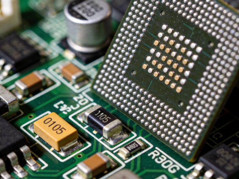
If you have ever spent hours debugging a prototype only to find out that your tiny 0201 resistors are standing straight up like little tombstones, you know the pain. Surface Mount Technology (SMT) is amazing, but it is unforgiving. Optimizing pad design to prevent tombstoning and bridging is one of the most important skills a Pcb designer can learn. It is not just about making the board look pretty; it is about ensuring high Manufacturing yield. In this article, I will share some practical insights from the assembly line on how to get your pad geometry right the first time.
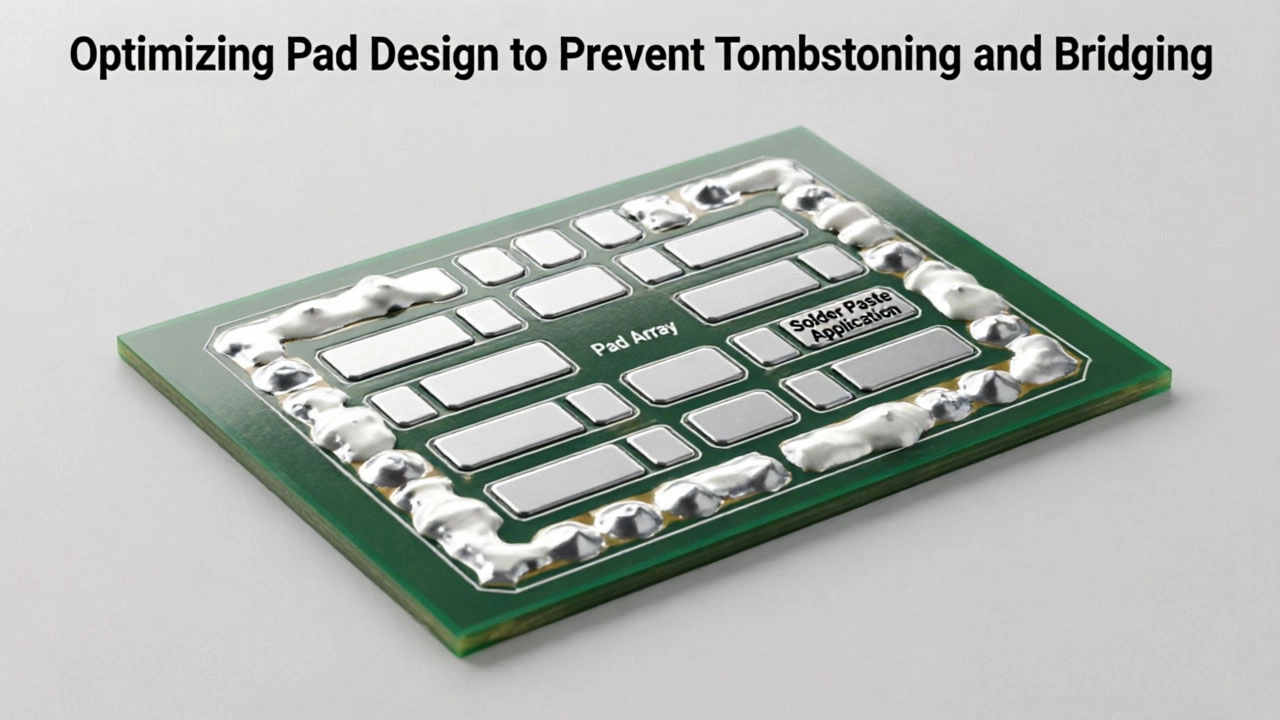
Before we fix the problem, we need to understand why it happens. Tombstoning occurs when one end of a chip component melts and solders before the other. The surface tension of the molten solder on the finished side literally pulls the component up into a vertical position. Bridging, on the other hand, is when solder connects two adjacent pads that should be isolated. This is usually caused by too much Solder Paste or pads that are too close together. When optimizing pad design to prevent tombstoning and bridging, you are essentially fighting against unbalanced thermal forces and fluid dynamics.
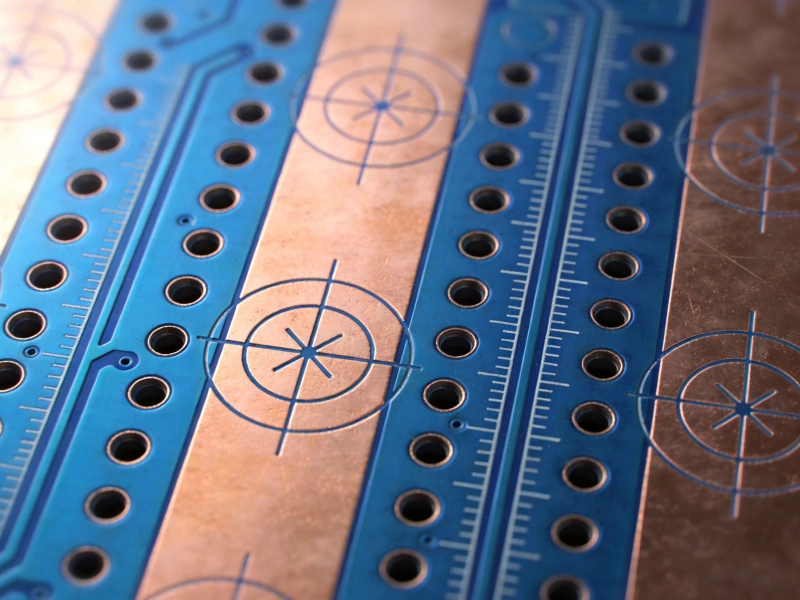
The single most effective way to stop tombstoning is to make your pads perfectly symmetrical. I cannot stress this enough. If the pad on the left is larger than the pad on the right, the larger pad will act as a heat sink. It will take longer to reach the reflow temperature, causing the smaller pad to solder first. Always use the IPC-7351 standard as your baseline. For a 0402 component, for example, your land pattern should be identical on both sides. Even a 0.05mm difference can be enough to cause issues at high reflow speeds. Symmetry ensures that both ends of the component heat up and melt at the exact same time.
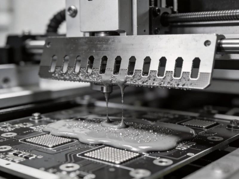
Bridging is often a volume issue. If your pads are as large as the component itself, you are asking for trouble. The Solder Paste will have nowhere to go when the component settles, so it squeezes out to the sides and shorts the pins. A good rule of thumb is to make the pad width slightly narrower than the component width. This creates a natural barrier that keeps the solder under the part. Also, consider using a solder mask defined pad. The solder mask acts as a physical dam, preventing the molten solder from spreading too far. When optimizing pad design to prevent tombstoning and bridging, less is often more.
How you connect the pad to the rest of the circuit matters a lot. If you have a thick copper trace going directly to one side of a resistor pad, that trace will suck the heat away during reflow. This creates a thermal imbalance, and guess what? Tombstoning. Always use a thermal relief pattern or a very thin trace for the first few millimeters. This allows the pad to heat up quickly and evenly. I have seen countless designs where engineers routed a power ground directly to a 0603 pad without any thermal relief, and the assembly house had to hand-solder every single board. Do not let your routing ruin your SMT process.
Pad design does not exist in a vacuum. The placement of components relative to each other is crucial. If you place a tall capacitor right next to a fine-pitch IC, the shadowing effect during reflow can cause uneven heating. Always maintain a proper keep-out zone around sensitive components. For bridging prevention, ensure there is enough solder mask dam between pads. A minimum of 0.1mm of solder mask between 0402 pads is usually safe. If you are designing for Automated Optical Inspection (AOI), giving the machine enough space to see the pad edges will also help catch defects early.
Optimizing pad design to prevent tombstoning and bridging is a mix of science and art. It requires respecting the physics of solder wetting and thermal transfer. By maintaining strict symmetry, controlling solder paste volume, managing thermal relief, and planning your layout carefully, you can dramatically improve your first-pass yield. Remember, fixing a pad in CAD takes five minutes; fixing it on a populated board takes hours. Take the time to get it right. If you have any questions about specific component footprints or reflow profiles, feel free to leave a comment below!
The Science of Solder Paste Printing: Stencil Design Best PracticesJune/17/2026
Panelization Strategies: V-Scoring vs. Tab Routing for Efficient DepanelingJuly/07/2026
Mastering DFM: Essential Design Rules for Flawless PCB AssemblyMay/22/2026
Fiducial Marks and Tooling Holes: Ensuring Precision in SMT PlacementJuly/15/2026

What is Reflow Soldering and Why Does the Temperature Profile Matter?July/14/2026

Cost-Reduction Strategies Without Compromising PCBA QualityJuly/09/2026

The Rise of AI Servers and Their Impact on HDI PCB AssemblyJuly/10/2026
Miniaturization Mastery: Handling 01005 Components and Micro BGAsJune/15/2026