

Large and thin PCBs present unique Manufacturing challenges that can compromise product quality and yield if not properly addressed. The physics of thin boards with substantial surface area creates susceptibility to warpage, handling damage, and assembly-induced stress that thicker boards handle without issue. Understanding these challenges and implementing appropriate solutions proves essential for successfully Manufacturing slim, large-format electronic products.
From smartphones to LED lighting panels, the demand for thinner, lighter products drives Pcb designs that push the limits of manufacturing capability. This guide examines the root causes of assembly stress in large thin boards and provides practical solutions for achieving reliable production outcomes.
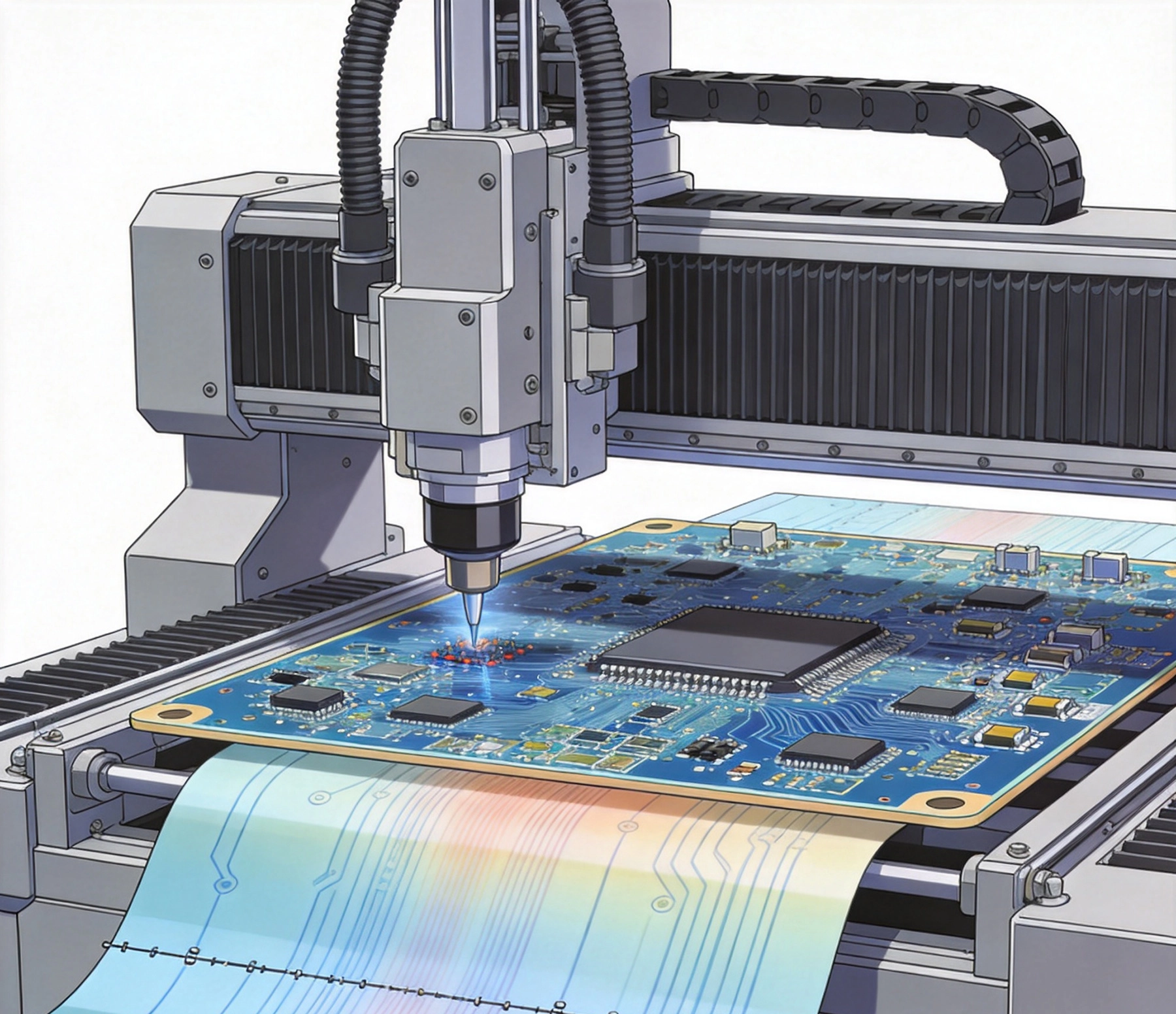
Warpage in large thin PCBs results from the complex interplay of thermal expansion, material properties, and manufacturing processes. Understanding these fundamental mechanisms helps designers and manufacturers implement effective countermeasures.
PCBs consist of multiple materials with different coefficients of thermal expansion (CTE). When subjected to temperature changes during assembly, these materials expand and contract at different rates, creating internal stresses that manifest as warpage.
The primary CTE mismatch occurs between:
In thin boards, this stress has less material thickness to distribute through, resulting in more pronounced warpage for the same thermal excursion.
During assembly, PCBs typically exist in panel formats before depanelization. The panelization approach significantly affects warpage behavior:
The constrained panel state during assembly differs substantially from the final free-state board, making prediction of field warpage challenging without proper process control.
Design decisions made early in the development process significantly impact manufacturing stress susceptibility. Implementing warpage-reducing design practices reduces downstream problems.
When product constraints allow, selecting appropriate board thickness provides the most fundamental solution:
If thinness is mandatory, alternative strategies must compensate for reduced stiffness.
Multi-layer board construction affects warpage tendency:
An asymmetrical stackup creates inherent bending tendency that thermal stress exacerbates. Always verify stackup symmetry during design review.
Copper distribution significantly affects warpage. Unbalanced copper creates stress gradients that drive bending:
Manufacturing processes can be adjusted to reduce stress on large thin boards. These modifications often involve trade-offs with throughput or cost but may prove necessary for challenging designs.
The reflow thermal profile significantly impacts warpage development. Consider these adjustments:
Profile optimization requires balancing warpage reduction against solder joint quality and throughput requirements.
Physical support during assembly provides immediate warpage control:
Fixtures must be designed for the specific board geometry and maintained to ensure consistent performance.
Panelization strategy affects manufacturing stress susceptibility:
Large thin boards face handling stress beyond thermal effects. Careful material handling protocols prevent damage throughout production.
Automation provides consistent handling that manual processes cannot match:
When manual handling is necessary, proper technique prevents damage:
Storage and transport carriers must provide adequate support:
Component placement affects stress distribution on thin boards. Strategic placement decisions reduce susceptibility to assembly-induced failures.
Heavy components create local stress concentration:
Pick-and-place machines must be configured appropriately:
Large component packages pose particular challenges:
Enhanced inspection helps identify stress-related defects before they reach customers.
Measuring warpage at critical process steps enables intervention:
Measurement methods include:
Some stress-related defects remain hidden until field failure:
Stress-related defects often manifest as field returns with intermittent symptoms, making prevention more valuable than detection.
Material choices made during design affect board stress behavior throughout manufacturing and field life.
Alternative base materials offer improved thermal stability:
Alternative materials typically cost more than standard FR-4 but may reduce total cost by preventing warpage-related yield loss.
Prepreg type affects lamination stress:
When warpage or stress issues occur despite prevention efforts, systematic troubleshooting identifies root causes.
Warpage occurring at different process stages indicates different causes:
Document when warpage is observed to narrow root cause investigation.
Frequent causes of assembly stress problems:
Solving assembly stress issues in large thin PCBs requires attention throughout the product lifecycle:
Large thin Pcb Manufacturing requires close collaboration between designers, manufacturers, and assemblers. Early communication about stress-sensitive designs enables appropriate process planning and fixture preparation.
Warpage in large thin PCBs results from thermal mismatch between different materials (copper, substrate, prepreg, solder) combined with insufficient board thickness to resist bending forces. Asymmetric copper distribution, improper thermal profiles, and handling stress compound the fundamental physics.
For PCBs larger than 100mm, 0.8mm minimum thickness provides reasonable handling capability. Boards larger than 200mm benefit from 1.0mm or thicker. If thinner boards are required, additional support, alternative materials, and modified processes become necessary.
Reduce warpage during reflow by slowing ramp rates to minimize thermal gradients, extending soak periods for temperature equalization, avoiding rapid cooling, using aluminum backing plates for thermal mass, and optimizing peak temperature to minimum acceptable levels.
Warpage can be measured using coordinate measuring machines for precision, optical flats for quick verification, and shadow moire interferometry for detailed stress analysis. Measure at incoming inspection, post-reflow, and final inspection stages.
Yes, component placement significantly affects stress distribution. Heavy components near board edges increase warpage tendency. Place heavy components near board center and distribute weight evenly. Consider adding stiffeners where heavy components mount.
Unbalanced copper creates asymmetric stress that drives bending. Copper on one side of the neutral axis but not the other creates residual stress. Balance copper weight on opposite layers, use copper thieving in sparse areas, and maintain consistent trace density across signal layers.
How to Reduce PCB Assembly Cost Without Sacrificing QualityOctober/22/2026
Designing for Testability (DFT): Placing Test Points for ICT and FCTJuly/31/2026
Silk Screen Best Practices: Improving Readability and Assembly EfficiencySeptember/15/2026
The Difference Between Quick Turn PCB Assembly and Standard ProductionOctober/16/2026
Understanding Prototype SMT Assembly China: A Step-by-Step GuideSeptember/26/2026
Panelization Strategies: V-Scoring vs. Tab Routing for Efficient DepanelingJuly/07/2026
Optimizing Pad Design to Prevent Tombstoning and BridgingJune/05/2026
Fiducial Marks and Tooling Holes: Ensuring Precision in SMT PlacementJuly/15/2026