Open Nav


Behind every Pcb that powers the devices you rely on, there's a story of engineering challenge and creative problem-solving. We believe the best way to demonstrate our capabilities isn't through marketing claims — it's by showing you what we've actually built, for whom, and how we solved the problems that made these projects difficult.
These aren't curated success stories with the hard parts edited out. Each project below faced genuine technical obstacles that required real engineering judgment, close collaboration with customers, and sometimes multiple design iterations before achieving a manufacturable solution. That's what Pcb Manufacturing partnerships are supposed to look like.

When a Boston-area medical device startup approached us, they had a novel continuous glucose monitoring concept and seed funding — but no established Supply Chain, no experience navigating FDA regulatory requirements, and a 24-month window to clinical trials that they needed to compress to 18. Their circuit board design was conceptually sound but entirely unmanufacturable at the cost targets their business model required.
The primary challenge was miniaturization. Their prototype used standard off-the-shelf components on a 6-layer rigid board — it worked on the bench, but the form factor was three times larger than what their clinical protocol required. We proposed migrating to an 8-layer HDI rigid-flex design with all passive components embedded in the substrate. This cut their board footprint by 65% and reduced assembly steps simultaneously.
The regulatory dimension added complexity that typical commercial projects don't face. Every component change required documentation for the FDA submission. We maintained a complete material and process change log throughout development, flagged potential issues early, and coordinated with their quality team on first-article inspection protocols. When their submission was reviewed, our Manufacturing records provided the traceability documentation their auditors needed.
Production launched on schedule with 500 units per month capacity, scaling to 5,000 monthly as clinical results came in positive. The startup closed their Series B six months after launch, citing Supply Chain readiness as a key investor confidence factor. Their device received FDA clearance and is now used in diabetes management programs across three states.
Early engineering involvement before the design was locked. The startup initially asked us to quote their existing design, but we recommended a design review engagement first. That review identified twelve components that were NRND (Not Recommended for New Designs) and three that would create single-source risks at production volumes. Catching these issues during design versus after board arrival saved them an estimated four months of potential delays.
A European EV charging network operator was experiencing field failures in their Level 2 charging stations that they couldn't trace to any obvious cause. Boards would fail after 6-12 months in the field — not catastrophic failures that left stations non-functional, but gradual degradation that increased charging times and triggered safety cutouts. Their original Contract Manufacturer had been replaced, and the new supplier's boards showed higher failure rates despite passing incoming inspection.
Root cause analysis revealed the problem: the new supplier was using standard FR4 material with a Tg (glass transition temperature) of 130°C. Their stations were installed in southern European climates where direct sun exposure could push internal temperatures above 100°C during summer afternoons. FR4 material approaching its Tg undergoes significant property changes, and the combination of Thermal Stress from temperature cycling and vibration from daily thermal expansion was degrading solder joints incrementally.
We specified high-Tg FR4 (Tg 170°C minimum) with enhanced thermal cycling ratings for all new production. We also redesigned the power delivery section using automotive-grade components rated for -40°C to +125°C operation, replacing commercial-temperature parts that were technically out of spec at their actual operating temperatures. Lead-free RoHS solder joints were re-qualified using thermal cycling profiles that matched their field conditions rather than standard laboratory profiles.
The re-engineered boards showed field failure rates below 0.3% annually across 8,000 deployed units — better than their original Manufacturing and well within their SLA requirements. The customer calculated that the reduced service call frequency saved approximately €180,000 annually in maintenance costs, and their network uptime improved to 99.7%.
The original boards passed standard quality tests but still failed in the field. This underscores a critical point: standard test conditions don't capture real-world deployment environments. We now ask every customer about their actual operating environment during design review, and we push back when designs specify commercial-grade parts for industrial or outdoor applications. The small cost premium for industrial or automotive-grade components almost always pays back through reduced field failures.
Commercial drone manufacturers face a fundamental trade-off: more electronics capability means heavier aircraft, which means shorter flight times. When a drone manufacturer developing a surveying drone asked us to help reduce their flight controller board weight by 30% without sacrificing reliability, it wasn't a simple optimization problem — it required rethinking nearly every aspect of their electronics packaging.
Their original board was a 4-layer rigid design with over 200 components including numerous discrete passives. We proposed migrating to an 8-layer HDI design with Embedded Passives in the core layers, replacing many discretes with integrated packages. This reduced the board area by 40% while maintaining the same functional capability.
Weight savings came from multiple sources simultaneously. The smaller board footprint allowed a smaller enclosure. The elimination of individual passive components removed their individual packaging weight. And the HDI construction with microvias allowed shorter routing that reduced trace lengths and enabled thinner dielectric layers, contributing to overall weight reduction without sacrificing signal integrity.
The final design achieved a 34% weight reduction compared to the original, with the total electronics package dropping from 85 grams to 56 grams. For a 2kg maximum takeoff weight drone, this weight savings translated directly to 14 minutes of additional flight time per charge — a 22% improvement that their customers immediately valued in surveying efficiency.
Structural testing revealed an unexpected benefit: the rigid-flex hybrid construction used for the daughterboard connections was more vibration-resistant than their original cable assemblies. Field reports showed a 40% reduction in vibration-related failures after the redesign, improving both reliability and customer satisfaction scores.
A Munich-based industrial automation company had a successful prototype for a wireless vibration sensor that monitored bearing health in manufacturing equipment. Their prototype worked beautifully — hand-assembled by their engineering team using premium components selected for performance rather than cost or availability. The problem: scaling to 50,000 units monthly required a completely different manufacturing approach than prototype assembly.
Component availability was the immediate crisis. Their prototype used 23 components that were either obsolete, allocation-restricted, or priced at spot-market premiums that would make their unit economics unworkable at volume. We spent three weeks doing a complete component redesign, identifying second-source equivalents for every critical part and qualifying alternate manufacturers for each.
The Pcb redesign optimized for automated assembly rather than hand assembly. Fine-pitch components were relocated to accessible positions with appropriate clearance for pick-and-place nozzles. Test points were added at key nodes to enable in-circuit testing that the prototype didn't require. We also specified tape-and-reel packaging for all automated placement, replacing the cut-tape and tube packaging common in prototypes.
Design For Manufacturing feedback identified thermal profile risks with their enclosure's internal temperature expectations. We worked with them to add thermal vias and copper pour areas that maintained component junction temperatures within rated limits even at the upper end of their -20°C to +85°C operating range specification.
Production launched at 10,000 units monthly and scaled to 50,000 within six months. First-pass yield exceeded 96%, and unit cost came in 23% below their prototype cost model. Their product is now deployed across 340 European manufacturing facilities, and they're developing a second-generation sensor that will share the same PCB platform with modifications for additional sensing modalities.
When a Hong Kong consumer audio company wanted to bring planar magnetic headphone technology to a mainstream price point, they faced the manufacturing challenges that typically make high-end audio expensive: tight tolerances, premium materials, and Quality Control processes that drive up cost. Their design goal was simple to state: audiophile-grade performance at $150 retail price.
The PCB challenge centered on their digital-to-analog converter (DAC) module. High-end audio DACs are sensitive to power supply noise, digital switching artifacts, and electromagnetic interference. Their original design used a standard 4-layer board with ground and power planes — adequate for the prototype, but the noise floor in their A/B listening tests showed distortion that would require expensive external filtering to address.
We redesigned their DAC module as a 6-layer board with dedicated analog and digital ground planes separated by an internal reference layer. Power supply routing isolated the analog section from digital switching noise, and we specified tight impedance control (±5%) on critical signal traces connecting to the DAC chip. The layout minimized return current loops and used guard traces around sensitive analog nodes.
Manufacturing process control was critical for this project. We implemented incoming inspection for all passive components in the analog signal path, matching capacitance values within 1% for the analog power supply filter network. Each production board received a noise floor measurement as part of standard test, rejecting any board that didn't meet their distortion specifications.
The production boards achieved a noise floor 18dB better than their prototype, and listening tests confirmed subjectively cleaner sound with better instrument separation. The headphones launched successfully and received positive reviews for build quality and sound performance, with reviewers noting the surprising quality at the price point. Monthly production of 8,000 units has maintained consistent quality across twelve production runs.
Agricultural technology companies face some of the harshest deployment environments in electronics: remote locations, extreme weather, and multi-year maintenance cycles that make battery replacement impractical. When a US agricultural technology firm needed soil moisture sensors for permanent installations in vineyards, their requirements were demanding: 10-year operational lifetime, solar/battery hybrid power, and communication reliability across rural areas with limited cellular coverage.
Power consumption was the make-or-break design parameter. Their prototype sensor consumed too much power, requiring battery replacement every 18 months — unacceptable for their customers and incompatible with their business model. We collaborated on a board redesign that cut microcontroller clock speeds during measurement cycles, implemented aggressive sleep modes between sensor readings, and added external watchdog circuits that could wake the system from deep sleep without consuming microcontroller power continuously.
The PCB itself had to survive environments that would destroy typical electronics: soil moisture, fertilizer chemicals, temperature swings from -30°C to +60°C, and UV exposure. We specified Conformal Coating on all boards, IP67-rated enclosures with appropriate cable sealing, and circuit protection components that would survive lightning-induced transients on the buried sensor cables.
Reliability validation used accelerated life testing: thermal cycling chambers cycling between temperature extremes, humidity chambers maintaining 95% RH at elevated temperature, and salt spray testing for deployments near coastal farmland. Boards surviving 2,000 thermal cycles and 1,000 hours of humidity exposure with no failures proceeded to field trials.
Field deployment began with 500 sensors across three vineyards. After 18 months, battery levels remained above 80%, and the solar charging system had proven reliable even through two winter seasons with reduced sunlight. Customer-reported communication reliability exceeded 99.2%, and the agricultural technology firm is now deploying sensors across an additional 12,000 acres with production scaling to 3,000 units monthly.
These six projects span different industries, complexity levels, and volume requirements — but they share patterns that characterize successful Pcb Manufacturing partnerships.
Early engagement beats late surprises. In every case, the earlier we became involved in the design process, the less costly the required changes were. A design review before tooling costs thousands of dollars. A re-tool after production starts costs tens of thousands and delays schedules by months.
Real environments matter more than standard conditions. Boards designed for laboratory conditions fail in real applications. Our most successful projects involve detailed conversations about how products will actually be used, stored, transported, and maintained — not just what datasheet specifications they must meet.
Manufacturing constraints shape good designs. There's no wall between design and manufacturing. The best designs account for how they'll be built, tested, and maintained. We routinely advise customers on design modifications that improve producibility without sacrificing performance — and we're honest when a design feature we could technically produce would create quality or reliability risks.
Documentation and traceability enable scaling. Every project that scaled from prototype to volume production succeeded because of good documentation. Complete BOMs, revision control, first-article inspection protocols, and process documentation aren't overhead — they're the foundation that makes volume production possible.
Whether you're developing your first embedded product or optimizing an established platform, we bring the same engineering focus to every project. The goal isn't just producing boards that pass incoming inspection — it's producing boards that succeed in your customers' hands over the full lifetime of your product.
At minimum: Gerber Files, BOM (with manufacturer part numbers), and a quantity/volume forecast. Better quotes include stack-up specifications, impedance control requirements, and test specifications. For complex designs, sharing your design intent and operating environment helps us identify potential manufacturing risks before we quote — which prevents costly surprises after production begins.
Design changes during active production are managed through formal ECO (Engineering Change Order) processes. We document each change, assess the impact on in-process boards and finished goods inventory, and coordinate timing with the customer. For urgent changes, we can often implement revisions within one production cycle while protecting existing inventory where possible.
Our facilities maintain ISO 9001 Quality Management certification, and we support customer-specific quality requirements including AS9100 (aerospace), Iatf 16949 (automotive), and IEC 62368 (safety-critical equipment). We work with customers on custom QA protocols for specialized applications including medical device, automotive, and military customers with unique requirements.
Yes. We've structured our production capabilities to handle both high-volume commodity boards and low-volume complex assemblies. Low-volume orders with high complexity face different economic realities than commodity production, and we're transparent about pricing structures so customers can make informed decisions about production strategies for their products.
We maintain active monitoring of component market conditions and proactively flag availability risks when we identify them during design review or BOM analysis. For production programs, we work with customers to establish buffer stock agreements for critical components and develop alternate sources before shortages become production-stopping problems.
Every project starts with listening. Tell us what you're building, what challenges you're facing, and what success looks like for your product. We'll tell you honestly what we can do, what it will cost, and what risks we see in your approach. That's the foundation for a manufacturing partnership that delivers results.
How We Handle Rush Orders and Quick-Turn PCB PrototypingJuly/08/2026
Our Quality Assurance Promise: AOI, X-Ray, and Functional TestingJune/26/2026
The Ultimate Guide to PCB Assembly Services in 2026September/24/2026
What to Expect from PCB Assembly Shenzhen SuppliersOctober/14/2026

Welcome to Our PCB Assembly Services Hub: Your Resource CenterMay/22/2026
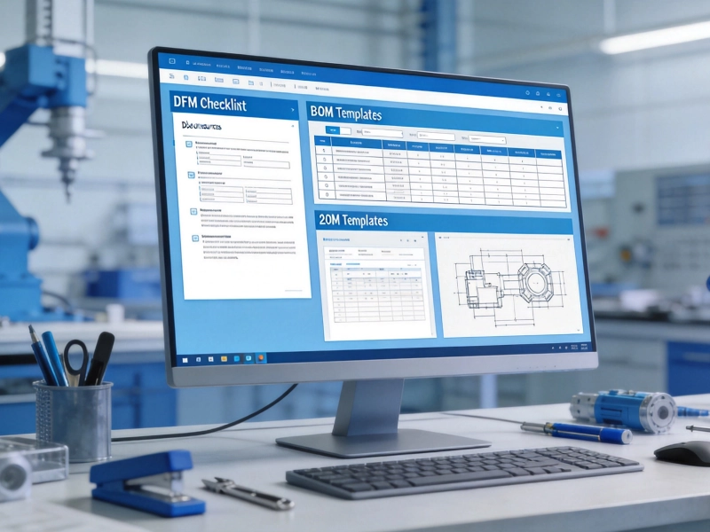
Downloadable Resources: DFM Checklists and BOM TemplatesAugust/03/2026
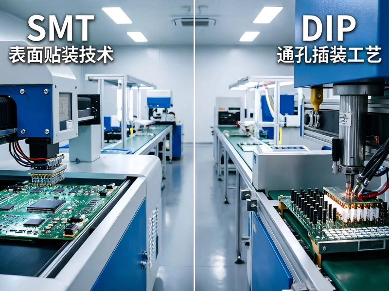
Comprehensive Guide to Our SMT and DIP CapabilitiesJune/09/2026
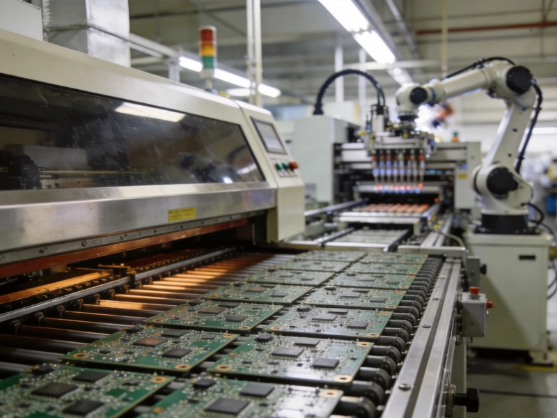
Frequently Asked Questions About Our PCB Assembly ProcessJuly/25/2026