
The relentless drive toward smaller, lighter, and more powerful electronic devices has pushed manufacturers to adopt increasingly miniature components. At the forefront of this miniaturization revolution are 01005 components and micro BGAs (Ball Grid Arrays), which represent some of the most challenging yet essential technologies in modern Electronics Manufacturing. These tiny components, measuring mere fractions of millimeters, enable the compact designs that consumers expect from today's smartphones, wearables, medical devices, and IoT products. However, handling and assembling these miniature marvels requires specialized equipment, refined processes, and deep expertise that separate capable manufacturers from those who merely claim to offer miniaturization services. This comprehensive guide explores the technical challenges, equipment requirements, process considerations, and best practices for successfully handling 01005 components and micro BGAs in high-volume Electronics Manufacturing.
The designation "01005" refers to the component's dimensions in inches: 0.01 inches long by 0.005 inches wide, which translates to approximately 0.4mm by 0.2mm. To put this in perspective, a single 01005 resistor is smaller than a grain of table salt and would easily pass through the eye of a sewing needle. Despite their microscopic size, these components must function reliably in demanding applications, withstanding thermal cycling, mechanical stress, and environmental exposure while maintaining precise electrical characteristics.
The adoption of 01005 components has accelerated dramatically as product designers seek to maximize functionality within increasingly constrained form factors. While 0402 components (1.0mm x 0.5mm) dominated portable electronics a decade ago, and 0201 components (0.6mm x 0.3mm) became common in the 2010s, 01005 components now represent the standard for space-constrained applications. This progression reflects both the relentless miniaturization of consumer electronics and the Manufacturing industry's ability to handle progressively smaller components with acceptable yields and reliability.
The electrical benefits of smaller components extend beyond mere space savings. Reduced lead inductance and resistance in 01005 components improve high-frequency performance, which is critical for RF circuits and high-speed digital interfaces. The smaller thermal mass enables faster reflow processing, reducing exposure time to high temperatures that can stress temperature-sensitive components and substrates. Additionally, shorter current paths in miniature components reduce parasitic effects that can compromise signal integrity in precision analog and high-speed digital circuits.
However, 01005 components present significant Manufacturing challenges that require careful attention to process control and equipment capabilities. The tiny mass of these components makes them susceptible to being displaced by air currents during placement, requiring controlled environments with minimal turbulence. Their small pad sizes demand precise Solder Paste application and accurate placement, with tolerances measured in microns rather than millimeters. Visual Inspection becomes extremely difficult, necessitating Automated Optical Inspection with high magnification and sophisticated image analysis algorithms.
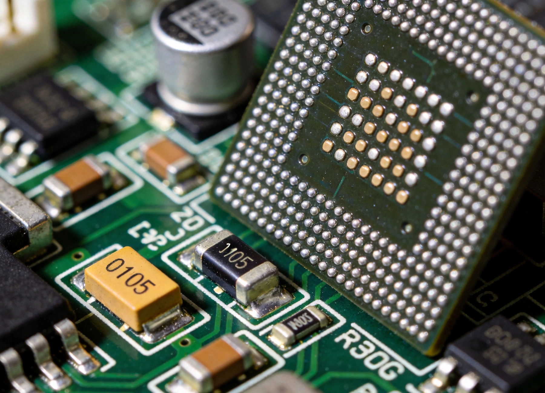
Micro BGAs represent another frontier in electronics miniaturization, offering high pin counts in compact packages with excellent thermal and electrical performance. Unlike traditional packages with leads extending from the perimeter, BGA packages feature solder balls arranged in a grid pattern on the underside of the component. This array configuration provides numerous advantages including shorter signal paths, better thermal dissipation, higher pin density, and improved mechanical reliability through solder joint coplanarity.
The term "micro BGA" typically refers to packages with ball pitches below 0.5mm and often below 0.4mm. Common micro BGA configurations include 0.4mm pitch packages with arrays ranging from 4x4 (16 balls) to 12x12 (144 balls), though larger arrays are increasingly common in complex integrated circuits. The extremely fine pitch and small ball diameters of micro BGAs present assembly challenges that demand specialized equipment and processes far beyond those required for larger BGA packages.
The thermal performance advantages of BGA packages make them particularly valuable for applications where heat dissipation is critical. The solder ball array provides multiple thermal paths from the component junction to the Pcb, enabling more efficient heat transfer than packages with perimeter leads. This thermal efficiency supports higher power densities and enables operation at higher frequencies and clock speeds without thermal throttling. For applications like graphics processors, network processors, and power management ICs, micro BGAs often represent the only viable packaging option for achieving required performance levels.
Electrical performance benefits stem from the short, uniform signal paths that the grid array provides. Each solder ball connects directly to the component's internal routing, eliminating the inductive and resistive variations that can occur in lead-based packages. This consistency is particularly valuable for high-speed differential signals where matched impedance is critical. The reduced package parasitics enable higher signal speeds and lower electromagnetic emissions, important considerations for wireless and high-speed digital applications.
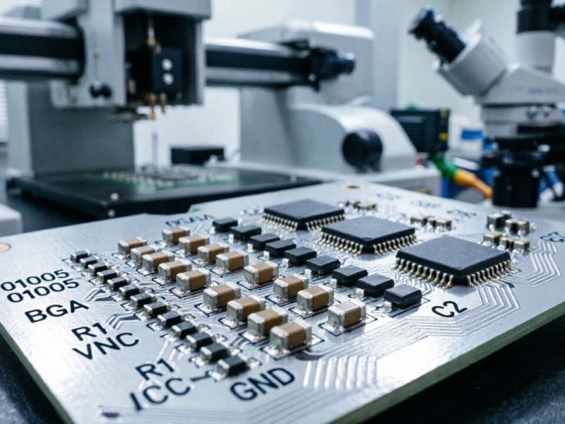
Successfully assembling 01005 components and micro BGAs requires equipment specifications that exceed those needed for conventional Surface Mount Technology. Manufacturing facilities must invest in precision placement systems, advanced inspection equipment, and process controls that maintain micron-level accuracy throughout the assembly process. Understanding these equipment requirements helps decision-makers evaluate manufacturing capabilities and identify potential limitations in their production processes.
Placement system requirements for 01005 components demand extraordinary precision and control. Modern high-speed placement machines capable of handling 01005 components must achieve placement accuracy of ±30μm (3 sigma) or better, with fine pitch packages requiring ±25μm accuracy. This precision necessitates advanced vision systems that can locate component features and Pcb fiducials with sub-pixel accuracy. Linear motor drives and precision mechanical systems minimize vibration and positioning errors that would compromise placement accuracy. Additionally, placement heads must provide controlled force application to prevent component damage while ensuring proper Solder Paste compression.
Solder Paste Printing equipment must deliver consistent paste deposition with volumes measured in nanoliters. Stencil technology has evolved to meet these requirements, with laser-cut stencils featuring increasingly fine aperture walls and advanced nano-coatings that improve paste release. Print alignment systems must achieve ±10μm registration accuracy to ensure proper paste placement on the correspondingly small pads. Automated Solder Paste Inspection (SPI) systems verify print quality in real-time, identifying defects before they propagate through subsequent assembly steps.
Reflow Soldering systems for miniature components require precise temperature profiling and controlled atmosphere options. The reduced thermal mass of 01005 components means they reach reflow temperatures faster than larger components, potentially creating temperature gradients within mixed-technology assemblies. Advanced profiling systems with high-density thermocouple placement verify that all components experience appropriate thermal profiles. Nitrogen atmosphere options reduce oxidation and improve solder wetting, particularly valuable for the small clearances between adjacent 01005 pads.
Inspection and test equipment must be capable of detecting defects invisible to conventional systems. Automated Optical Inspection (AOI) systems require magnification capabilities exceeding 100x and sophisticated lighting schemes that reveal defects in highly reflective miniature solder joints. For micro BGAs, X-ray inspection becomes essential, as the solder balls beneath the package are completely hidden from optical view. 3D X-ray systems and computed tomography (CT) scanning enable detailed inspection of internal solder joint quality and void detection.
Equipment capability alone does not guarantee success with 01005 components and micro BGAs; process optimization is equally critical. Fine-tuning each step of the assembly process ensures consistent quality and acceptable yields at production volumes. Experienced manufacturers develop and refine processes over time, building institutional knowledge that enables reliable production of challenging miniature assemblies.
Solder paste selection requires careful consideration of particle size, flux chemistry, and rheological properties. Type 6 or Type 7 solder powder (with particle diameters of 5-15μm and 2-11μm respectively) is typically required for 01005 components to ensure proper paste release from stencils. The flux system must provide adequate cleaning action without leaving residues that could cause reliability issues. For micro BGAs, void-free solder joints are often critical, requiring low-voiding flux chemistries and optimized reflow profiles that promote bubble escape.
Stencil Design optimization directly impacts paste deposition quality for miniature components. Aperture size and shape must balance paste volume requirements against release characteristics. Typically, 01005 apertures use reduced area ratios compared to larger components, often 0.5-0.6 rather than the traditional 0.66 minimum. Aperture corner radius and wall smoothness affect paste release, with electropolished laser-cut stencils generally providing superior performance. Step-down stencils may be appropriate when mixing 01005 components with larger parts, providing thinner deposits where needed for miniature components while maintaining adequate volume for larger pads.
Placement optimization involves balancing speed against accuracy and component protection. While modern placement systems can achieve remarkable speeds, production of 01005 components may require reduced placement rates to maintain accuracy and prevent component damage. Vacuum pickup force must be carefully controlled—insufficient vacuum allows components to drop or misalign, while excessive force can crush delicate components or cause them to flip. Head-to-board approach speed and placement force profile require optimization for each component type.
Reflow profile development for mixed assemblies containing both 01005 components and larger parts requires careful balancing of thermal requirements. The small mass of 01005 components means they heat and cool faster than larger components, potentially creating temperature overshoot during ramp stages. Soaking zones may need adjustment to ensure adequate time for flux activation while avoiding excessive thermal exposure. Peak temperature, time above liquidus, and cooling rate must all be optimized considering the requirements of all component types present on the assembly.
Quality assurance for 01005 components and micro BGAs demands more comprehensive inspection and testing than conventional assemblies. The small size of these components makes defects harder to detect, and the high-density assemblies they enable limit access for repair. Establishing robust quality assurance protocols ensures that defective assemblies are identified and addressed before they reach customers.
Statistical Process Control (SPC) becomes essential for maintaining quality in miniature component assembly. Monitoring key process parameters including paste print volume, placement accuracy, and reflow profile characteristics enables early detection of process drift before it results in defective assemblies. Control charts and capability analysis help maintain process capability at the levels required for reliable miniature assembly. Many manufacturers implement real-time SPC systems that automatically adjust process parameters when trends indicate potential issues.
Defect detection strategies must address the unique challenges of miniature components. For 01005 assemblies, common defects include Tombstoning (where one end of a component lifts while the other solders properly), skewing (rotation from correct orientation), insufficient solder, and Solder Bridging between adjacent pads. AOI systems must be configured with inspection criteria that balance sensitivity against false call rates, often requiring multiple inspection angles and lighting conditions to detect all defect types reliably.
Micro BGA inspection presents unique challenges due to the hidden nature of solder joints. X-ray inspection is mandatory for detecting defects such as voids, insufficient solder, misregistration, and cracked joints. 2D X-ray provides quick screening capability, while 3D laminography or computed tomography enables detailed analysis of specific joints suspected of problems. Cross-sectional analysis of sample assemblies provides destructive verification of joint quality and metallurgy.
Environmental stress testing validates the reliability of miniature component assemblies under conditions they may encounter in actual use. Temperature cycling, thermal shock, mechanical vibration, and humidity exposure testing reveal weaknesses that may not appear during normal inspection. These tests are particularly important for automotive, medical, and aerospace applications where failure could have serious consequences. Failure analysis of stressed samples provides insights that enable targeted process improvements.
Manufacturers encounter numerous challenges when working with 01005 components and micro BGAs. Understanding these challenges and their solutions helps both manufacturers and their customers navigate the complexities of miniature assembly. Experience-based solutions developed through countless production builds provide valuable guidance for addressing recurring issues.
Component handling and storage represent fundamental challenges for 01005 components. The extremely small size makes components susceptible to being displaced by air currents, static charge, or vibration. Proper storage in sealed moisture barrier bags with desiccant protects components from moisture absorption while preventing loss. Handling procedures must minimize exposure to uncontrolled environments and prevent contamination from skin oils or particles. Tape-and-reel packaging with appropriate pocket dimensions ensures that components present correctly for automated placement.
Solder bridge formation between adjacent 01005 pads is a common defect that requires attention to multiple process factors. Insufficient paste volume, excessive paste spread, component placement accuracy errors, and uncontrolled reflow can all contribute to bridging. Addressing these factors through stencil optimization, placement accuracy improvement, and profile tuning typically resolves bridging issues. In extreme cases, increasing pad spacing or adjusting component orientation may be necessary design changes.
Tombstoning of 01005 components occurs when uneven heating or wetting causes one termination to solder while the other lifts. This defect is often related to pad size asymmetry, uneven Solder Paste Deposition, or thermal gradients during reflow. Balancing pad sizes, improving print uniformity, and optimizing reflow profile thermal balance address most tombstoning issues. Component supplier variation can also affect tombstoning tendency, making component qualification important.
Micro BGA voiding remains a persistent challenge despite advances in materials and processes. Voids can weaken solder joints and potentially cause failure under thermal or mechanical stress. Low-voiding solder pastes, optimized reflow profiles with controlled nitrogen atmosphere, and proper Stencil Design all contribute to void minimization. X-ray inspection quantifies void percentages, with acceptance criteria typically limiting void size and percentage based on application requirements.
Rework of miniature components presents significant challenges due to limited access and thermal sensitivity. 01005 components may require microscopes or high-magnification video systems for visual manipulation, while micro BGAs require specialized rework equipment capable of applying localized heat while protecting surrounding components. Establishing capability for miniature component rework requires investment in specialized equipment and extensive operator training.
Successful miniaturization begins with design decisions that support manufacturing requirements. Collaboration between design engineers and manufacturing teams ensures that designs incorporate features that enable reliable, manufacturable assemblies. Following established design guidelines for miniature components dramatically improves first-pass yield and long-term reliability.
Pad Design for 01005 components must balance solderability requirements against density needs. Recommended pad dimensions typically target 0.22-0.24mm length with 0.12-0.14mm width for standard 01005 resistors and capacitors, though exact dimensions vary by component and application requirements. Pad spacing must accommodate solder bridge prevention while maximizing density. Solder mask defined pads generally provide better accuracy than copper defined pads for miniature assemblies.
Via placement relative to surface mount pads requires careful consideration in miniature designs. Buried vias beneath pads can affect solderability and joint reliability. Via-in-pad techniques must be carefully designed to prevent solder wicking into vias that could cause insufficient solder volume. When vias are required near pads, tenting or plugging prevents solder flow into holes while maintaining surface planarity.
Component spacing guidelines ensure adequate clearance for assembly and inspection processes. Minimum spacing between 01005 components should typically be at least 0.15-0.2mm, though tighter spacing may be possible with optimized processes. Components should maintain clearance from board edges, mounting holes, and other features to facilitate handling during manufacturing. Higher-density designs may require longer development cycles to establish reliable processes.
Thermal design considerations become more critical in high-density miniature assemblies. The compact placement that miniaturization enables can create thermal concentration that stresses components and solder joints. Thermal relief strategies, ground planes, and thermal vias help distribute heat and prevent hot spots. For power components, dedicated thermal pathways may be essential to maintain acceptable junction temperatures.
Miniaturization through 01005 components and micro BGAs represents both an opportunity and a challenge for electronics manufacturers. The ability to assemble these microscopic components reliably enables product designs that would be impossible with larger packages, opening new possibilities for compact, feature-rich electronic products. However, realizing these benefits requires substantial investment in equipment, process development, and expertise that go far beyond conventional Surface Mount Assembly.
Success with miniature components demands attention to every aspect of the assembly process, from component storage and handling through solder paste application, placement, reflow, and inspection. Each step presents unique challenges that require optimization and tight process control. Manufacturers who master these challenges position themselves to serve the most demanding applications in medical devices, aerospace, Automotive Electronics, and cutting-edge consumer products.
The continued trend toward miniaturization shows no signs of slowing. As components become even smaller and packages more complex, manufacturers must continue advancing their capabilities to remain competitive. Investment in equipment, process development, and skilled personnel today prepares organizations for the miniaturization challenges of tomorrow. By understanding the requirements for handling 01005 components and micro BGAs, engineers and decision-makers can make informed decisions about manufacturing capabilities and partnership opportunities.
Modern high-volume manufacturing can reliably assemble components down to 008004 size (0.2mm x 0.1mm), though 01005 (0.4mm x 0.2mm) remains the practical minimum for most production environments. The choice depends on equipment capabilities, process maturity, yield requirements, and cost considerations. While smaller components may be technically assemblable, the cost and complexity may not justify benefits for most applications.
Properly assembled 01005 components can achieve reliability equal to or exceeding larger components when processes are properly optimized. The smaller solder joint size means mechanical stress per unit area may be higher, but the reduced thermal mass and improved thermal cycling characteristics often compensate. Reliability Testing specific to the application environment should validate assembly robustness.
Essential equipment for micro Bga Assembly includes precision placement systems with advanced vision capabilities, high-resolution Solder Paste Printing systems, advanced reflow ovens with precise temperature control, X-ray inspection systems for hidden joint verification, and 3D AOI systems for comprehensive defect detection. Additional equipment for process development and failure analysis may include cross-sectioning equipment, scanning acoustic microscopy, and Thermal Profiling systems.
Cost reduction strategies include designing for maximum producibility to reduce process complexity, using standard component sizes and packages where possible, establishing long-term relationships with suppliers for volume pricing, and investing in process development to improve yields. While miniature components may have higher unit costs, the overall product cost may decrease when considering board size reduction and integration benefits.
Common defects include Solder Bridging between adjacent pads, tombstoning where components lift at one end, insufficient or excessive solder, component skew or rotation, voids in BGA solder joints, and misregistration between component and pad. Advanced inspection systems and tight process control address these defects, with root cause analysis guiding continuous improvement efforts.
Embedded Component Technology: The Future of Ultra-Compact BoardsJuly/29/2026
Handling 01005 Components and Micro BGAsJune/03/2026

AI-Driven Manufacturing: How Smart Factories are Improving PCBA YieldJuly/02/2026

Flexible and Rigid-Flex PCBs: Meeting the Demand for WearablesJuly/21/2026

Top 5 PCB Assembly Trends Shaping the Industry in 2026May/22/2026

The Evolution of Digital Twins in PCB Assembly Process ControlJuly/13/2026
Bridging the Gap Between R&D Prototypes and Stable Mass ProductionJuly/27/2026

How Automotive Electronics are Redefining PCBA Quality StandardsJuly/01/2026