Open Nav

In the relentless pursuit of sleeker smartphones, smarter wearables, and powerful AI edge devices, printed circuit boards have transformed into microscopic cities. Today, engineers are routinely packing components smaller than a grain of sand onto densely populated boards. But as we push the boundaries of physics, the Manufacturing process becomes exponentially more unforgiving. So, how do top-tier factories achieve near-perfect yields when dealing with parts that have virtually zero tolerance for error?
This article explores the technical realities of miniaturization mastery. We will examine the specific engineering challenges and proven solutions involved in handling 01005 passives and micro Ball Grid Arrays (BGAs), providing actionable insights for design engineers and Manufacturing partners alike.
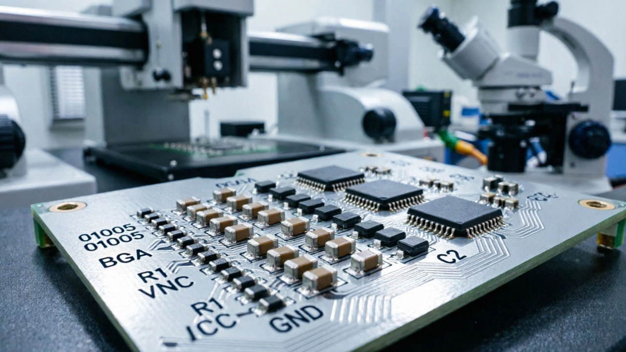
The 01005 package measures a mere 0.4mm by 0.2mm. At this scale, standard SMT processes fail rapidly. A slight misalignment of just 50 micrometers can easily result in Tombstoning or open circuits. Furthermore, these components weigh practically nothing—often less than a milligram—making them highly susceptible to shifting during the liquid phase of soldering.
Practical Takeaway: If your design includes 01005s, avoid placing them directly adjacent to large thermal sinks or heavy BGA packages. The differing thermal masses can cause severe localized temperature gradients during reflow, leading to consistent alignment failures.
While 01005s test our mechanical limits, micro BGAs (with pitches of 0.3mm or less) and Package-on-Package (POP) architectures test our metallurgical and inspection capabilities. With solder balls hidden beneath the component body, traditional optical inspection is entirely useless.
From my experiance reviewing production data at high-end PCBA facilities, I've noticed that environmental stability is just as critical as machine calibration. Even minor fluctuations in factory humidity can alter Solder Paste viscosity, causing catastrophic printing defects on micro-BGA pads.
You cannot manage what you cannot measure. Miniaturization demands a shift from reactive quality checks to proactive, closed-loop manufacturing.
Furthermore, 3D AOI (Automated Optical Inspection) uses phase-shift technology to measure the actual physical height and volume of solder fillets on 01005s, effectively eliminating false calls caused by shadow effects or reflective surfaces common in dense layouts.
Mastering the assembly of 01005 Components and micro BGAs is not about finding a single magic bullet; it requires a holistic ecosystem approach. It demands flawless DFM collaboration, state-of-the-art equipment, rigorous environmental controls, and statistical process discipline. When these elements align, manufacturers can confidently push the boundaries of electronic miniaturization.
Struggling with yield issues on your next ultra-dense board? Stop guessing and start optimizing. Contact our engineering team today for a comprehensive Design for Manufacturing (DFM) audit tailored specifically for micro-component assembly.
Q1: What is the minimum safe spacing between an 01005 and a micro BGA?
Generally, maintaining a clearance of at least 0.15mm to 0.2mm is recommended to prevent Solder Bridging during reflow, though this depends heavily on your specific Pad Design and stencil aperture ratio.
Q2: Can standard Type 3 Solder Paste be used for 01005s?
No. Type 3 powder is too coarse and will cause inconsistent deposition and bridging. You must use Type 4 or Type 5 solder paste, which features finer particle sizes (20-38μm) essential for fine-pitch printing.
Q3: How do you prevent Tombstoning on 01005 resistors?
Tombstoning is usually caused by unbalanced wetting forces. Ensure symmetrical pad designs, uniform paste deposition, and a controlled reflow ramp rate so both ends of the component melt simultaneously.
The Evolution of Digital Twins in PCB Assembly Process ControlJuly/13/2026
Miniaturization Mastery: Handling 01005 Components and Micro BGAsJune/15/2026

Top 5 PCB Assembly Trends Shaping the Industry in 2026May/22/2026

Flexible and Rigid-Flex PCBs: Meeting the Demand for WearablesJuly/21/2026

AI-Driven Manufacturing: How Smart Factories are Improving PCBA YieldJuly/02/2026
What is Reflow Soldering and Why Does the Temperature Profile Matter?July/14/2026
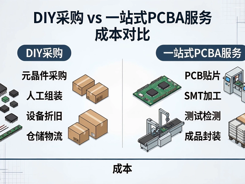
The Hidden Costs of DIY Sourcing vs. Turnkey PCBA ServicesJune/08/2026
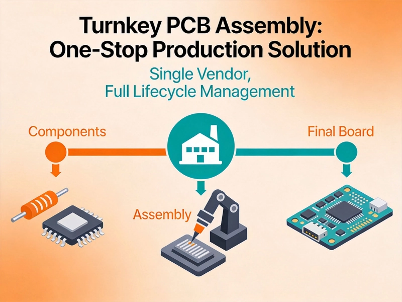
Why Choose Turnkey PCB Assembly for Your Next Product Launch?May/22/2026