
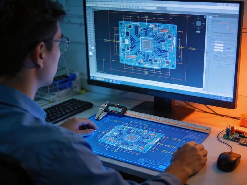
Every generation of consumer electronics seems to come with the same announcement: thinner, lighter, more powerful, longer battery life. What listeners rarely hear is what made it possible—or the quiet engineering battle that had to be won to pack that much performance into a chassis that fits in your pocket. The answer, more often than not, involves High-density Interconnect—HDI—PCBs. And HDI doesn't just change the board design. It changes every single step of how that board gets assembled. Getting it right requires understanding challenges that simply don't exist in conventional Pcb Assembly, and solving them with precision that borders on the obsessive.
Let's start with what HDI actually means in Manufacturing terms, because the term gets used loosely and the difference matters for assembly. HDI PCBs are characterized by higher wiring density than conventional boards—finer lines and spaces, denser component packing, and crucially, the use of micro-vias instead of through-holes for interlayer connections. These micro-vias are typically laser-drilled, with diameters of 0.1mm or less. Some advanced HDI designs use blind and buried vias with sequential lamination, meaning the board is built up in layers with connections made at specific intermediate points rather than running through the entire stack.
The assembly implications are significant. When your pad pitch drops from 0.5mm to 0.3mm or finer, your Solder Paste volume tolerances tighten dramatically. When you're placing 0.3mm × 0.3mm chip components next to fine-pitch BGAs with 0.4mm ball pitch, your placement accuracy requirements go from "very good" to "extraordinary." When your board has 10, 12, or 16 layers with blind micro-vias, your thermal management during reflow becomes a completely different problem than it is for a 4-layer through-hole board. None of these are insurmountable. But they're all significantly harder than standard assembly—and they interact in ways that can catch an unprepared team off guard.
At standard SMT pitches—0.5mm and above—a stencil's thickness variation and print alignment contribute some percentage to defect rate, but the process is forgiving enough that good equipment and reasonable process controls produce excellent first-pass yields. HDI changes this calculus entirely.
When you're printing Solder Paste for 0.4mm pitch BGA packages, the pad dimensions are approximately 0.2mm × 0.2mm. The stencil aperture for this pad might be 0.18mm × 0.18mm, with a thickness of 0.08mm or less. The paste volume that deposits on that pad—and the uniformity of that volume across a board with hundreds or thousands of similar apertures—is now operating at tolerances measured in thousandths of a millimeter. Contamination on the stencil, slight squeegee pressure variations, or substrate warpage that you'd never notice on a standard board can cause catastrophic solder defects at HDI scale.
Laser-cut stainless steel stencils with nanometer-level aperture smoothness. Electroformed nickel stencils for the most demanding applications where aperture quality directly drives yield. Closed-loop print inspection systems that measure actual paste volume post-print and reject boards before placement if volume falls outside specification. And critically—regular stencil maintenance protocols. In HDI work, a stencil that's been used for 500 prints without cleaning isn't the same stencil that was new.
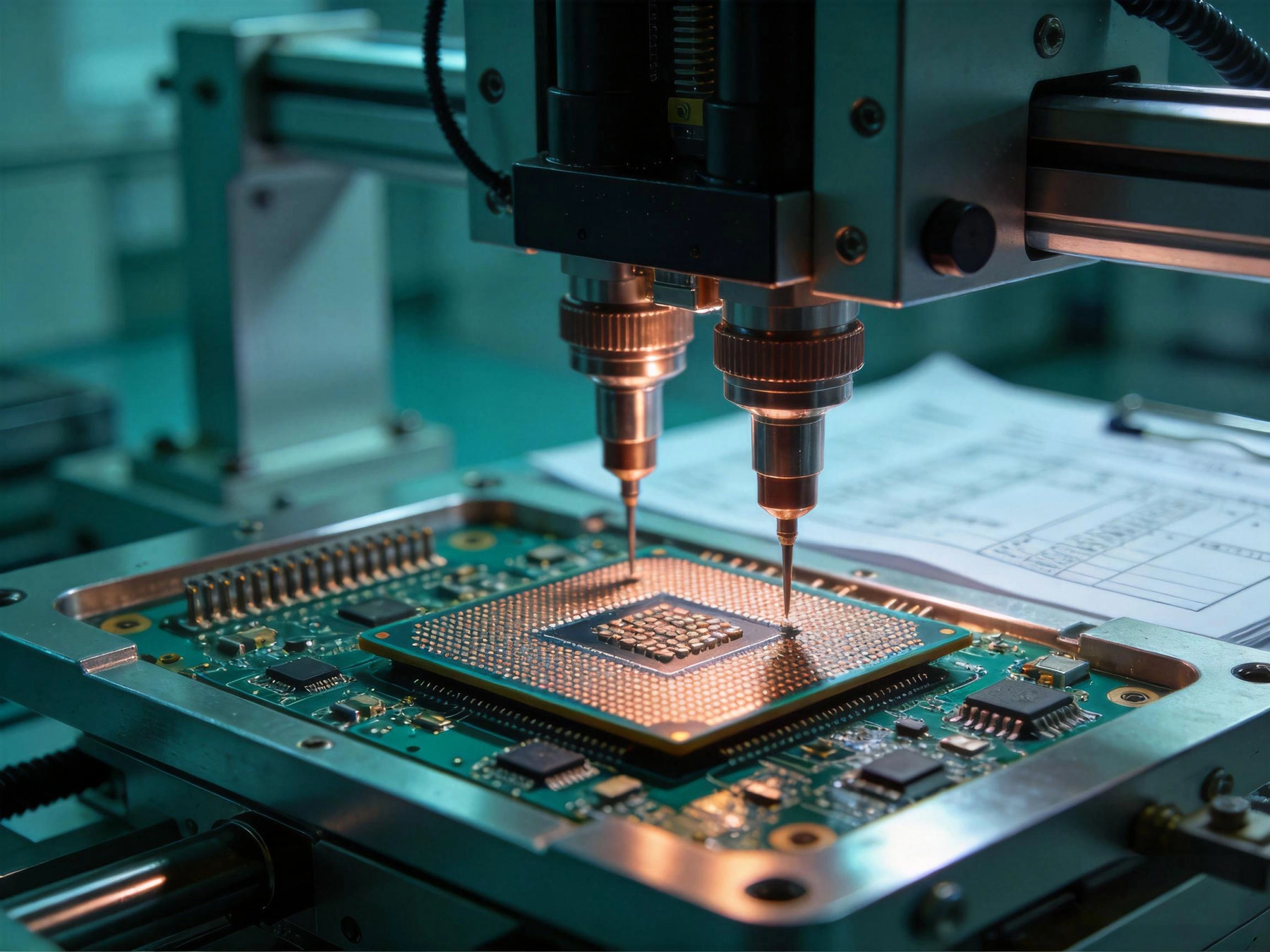
Modern pick-and-place equipment is genuinely impressive. High-end machines achieve placement accuracy of ±0.025mm at 3-sigma for standard components. But "standard components" covers a lot of ground, and the numbers change fast when you move to fine-pitch and micro components.
A 0.3mm pitch BGA with 0.4mm ball pitch—increasingly common in application processors, memory devices, and communication chips—has a total positional error budget of perhaps ±0.05mm including self-alignment during reflow. That sounds like a lot until you calculate what happens at 0.4mm pitch: a placement error of 0.06mm puts a ball entirely off its pad. The self-alignment forces in reflow can compensate for some offset, but only up to about half a ball diameter. Past that, you get bridging, opens, or Tombstoning.
For the smallest chip components—0201m (0.25mm × 0.125mm) and 01005 (0.4mm × 0.2mm)—the challenge shifts from ball pitch to pad size. These parts are physically tiny, which means they're light, which means they can be displaced by air currents in the pick-and-place head, by vibration, by electrostatic attraction to the nozzle, or by the momentum of the placement head deceleration. The margin for error collapses toward zero.
Vision systems are everything in HDI placement. Advanced machines use multiple fiducial recognition—global fiducials for board offset correction, local fiducials for component-specific correction, and laser or structured-light 3D measurement for coplanarity verification. Nozzle selection becomes critical: softer carbon-fiber nozzles for sensitive parts, dedicated nozzles sized exactly to each component, and frequent nozzle inspection and replacement schedules. Feeder precision matters too—part positioning in the tape must be verified before pickup.
Automated Optical Inspection—AOI—is a reliable workhorse for conventional Pcb Assembly. It catches Missing Components, gross solder defects, and orientation errors effectively. For HDI assemblies, AOI hits a wall when the joints you're trying to inspect are smaller than the optical resolution of the system, or when they're hidden under BGAs, QFNs, or other area-array packages.
Consider a 0.4mm pitch BGA. Each solder ball joint is approximately 0.25mm in diameter. The gap between joints at 0.4mm pitch is 0.15mm. AOI systems operating at standard resolution may be able to see this joint, but they can't reliably inspect what's happening inside it—the intermetallic formation, the voiding, the true quality of the metallurgical bond. And for BGAs, QFNs, and LGAs, the joint is entirely hidden under the component body. AOI can't see under the chip. Nothing optical can.
The inspection gap in HDI assembly is where defects hide and escape to the field. A BGA with 20% voiding in its solder joints may pass visual inspection and functional test in the factory—and then fail in the customer's hands after thermal cycling. The factory test caught the wrong thing because they weren't looking at the right failure mode.
X-ray inspection is non-negotiable for HDI assemblies with area-array packages. 2D X-ray reveals voiding, bridging, and solder volume inconsistencies. 3D X-ray CT scanning (used selectively on cross-section samples and failure analysis) reveals true joint quality including hidden cracks and delamination. Beyond X-ray: 3D AOI systems with structured-light projection that can measure solder volume and joint height, not just appearance. And acoustic micro-imaging for delamination detection in the board substrate itself—critical for multilayer HDI boards where interlayer voids can be catastrophic.
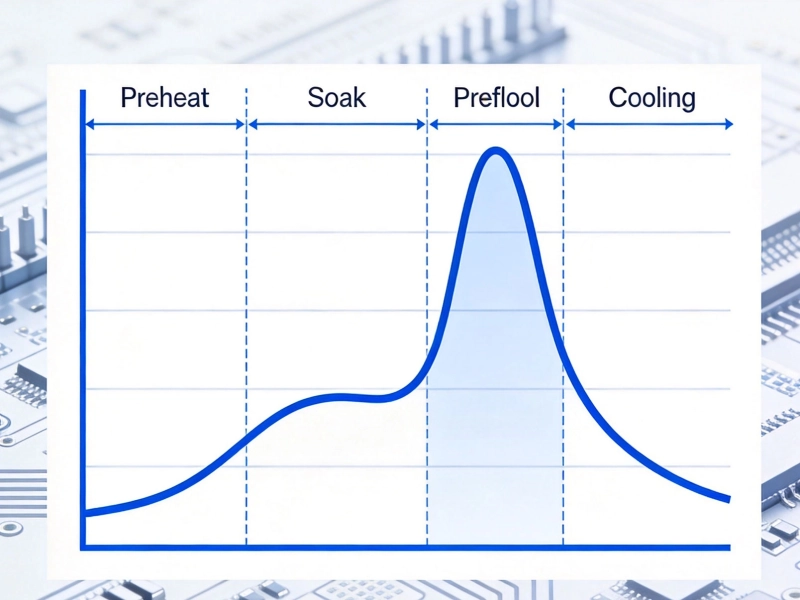
Reflow Soldering is a controlled thermal process: the board and its components move through a Temperature Profile that melts solder paste and forms permanent joints. For standard assemblies, this profile is well-characterized and forgiving. For HDI assemblies, the thermal dynamics become considerably more complex.
The primary complication is layer count and material stack. A 12-layer HDI board has significantly different thermal mass and thermal conductivity characteristics than a 4-layer standard board. The thick copper planes and dielectric layers conduct and distribute heat differently. Blind micro-vias create thermal pathways that don't exist in through-hole designs—sometimes concentrating heat in unexpected ways, sometimes acting as thermal barriers. Some HDI boards include materials beyond standard FR-4—high-Tg substrates, polyimide layers, metal cores—which all have different thermal requirements.
The consequences of getting the reflow profile wrong scale with density. On a standard board, a profile that's slightly off might produce a few joints with insufficient solder or minor voiding—defects that show up at test. On an HDI board with dense BGA arrays, the same profile error might produce a cascade of joint failures across an entire component, or warpage that shifts component positions beyond the self-alignment window. Neither outcome is acceptable at the volumes HDI assemblies typically serve.
Every HDI build requires a custom thermal profile developed through empirical measurement, not generic "recommended" profiles from paste manufacturers. This means placing thermocouples at multiple locations across the board—including at the highest-density component locations—and running profile boards through the reflow oven with actual paste to measure real thermal behavior. For complex stack-ups, use simulation tools to model heat distribution before running production. And consider nitrogen atmosphere reflow: oxygen in the reflow environment contributes to oxidation and uneven heating that is especially problematic for fine-pitch HDI joints.
Board warpage is the nemesis of fine-pitch assembly. When a board warps during reflow—due to mismatched CTE between layers, uneven heating, or insufficient backing—it lifts at the corners while the center stays hot, or vice versa. At standard pitches, this warpage is usually within the self-alignment correction window. At HDI pitches, it frequently isn't.
The problem is especially acute for HDI boards because their construction—thin dielectrics, high copper weights in inner layers, laser-drilled micro-vias—creates inherently stress-concentrated structures. A board that's flat at room temperature may warp during the thermal excursion of reflow, and the warpage during reflow is what determines joint quality, not the flatness at room temperature. Testing warpage with a board that's cooled to room temperature tells you only part of the story.
The consequences of warpage go beyond cosmetic defects. Warped boards can cause Tombstoning for small chip components—where one end of a component lifts during reflow while the other stays soldered, leaving an open joint. For BGAs, warpage can shift the component relative to the pads by amounts that exceed self-alignment correction, creating opens or bridges. In extreme cases, warpage during lamination causes delamination within the board stack—interior failures that are nearly impossible to detect post-build and can cause field returns months after assembly.
Warpage control starts at fabrication: high-quality HDI manufacturers use lamination processes with precise temperature and pressure control, copper foil weight balancing across the stack, and post-lamination stress relief procedures. During assembly, thermal warpage is managed through careful profiling (as mentioned above), support fixtures for boards that are prone to warp during reflow, and panelization strategies that minimize the stress introduced by the depanelization process. For critical applications, 3D scanning of boards pre- and post-reflow provides data to correlate warpage with defect rates and identify which board lots need special handling.
Standard Pcb rework is a known process: hot air rework station, careful temperature profiling, flux application, and a skilled technician. The tolerance for error is relatively forgiving—a slightly high temperature might discolor the solder mask but won't destroy the board. The same is not true of HDI rework.
HDI boards are more thermally sensitive and mechanically delicate than standard boards. The micro-via structure is susceptible to damage from excessive heat. The high layer count means there are more interfaces where delamination can initiate. The fine traces and small pads mean that any movement or misalignment during component removal or replacement is more likely to cause permanent damage. And the dense component placement means that accessing a component in the middle of a dense area—without affecting adjacent components—requires precision tooling and technique that standard rework doesn't demand.
Perhaps most critically: a component removed from an HDI board for rework may take the pads with it. At 0.3mm pitch and below, the pad is so small and the solder interface so constrained that the removal forces required to lift a BGA can exceed the adhesion strength of the pad-to-laminate bond. The component is now off the board, but so are several pads, and the board may be more damaged than it was before the rework attempt.
BGA rework stations with closed-loop temperature control and vacuum pickup for components—don't use tweezers for HDI component removal. Bottom-side preheating to reduce thermal gradients across the board during rework. Flux application optimized for rework (higher-activity formulations than production paste). And critically: a thorough incoming inspection process and process controls good enough that rework is the exception, not the rule. In high-quality HDI assembly, the rework rate should be under 0.5% for all defects found at inspection—and defects escaping to rework should be far lower still.
| Parameter | Standard Pcb Assembly | Hdi Pcb Assembly |
|---|---|---|
| Minimum pitch | 0.4mm–0.5mm typical | 0.2mm–0.3mm fine pitch |
| Via type | Through-hole + mechanically drilled blind/buried | Laser micro-vias (0.1mm or less) |
| Stencil thickness | 0.1mm–0.15mm typical | 0.05mm–0.08mm, often below 0.1mm |
| Placement accuracy required | ±0.05mm to ±0.08mm | ±0.025mm or tighter |
| Inspection method | Standard AOI sufficient for most | 2D/3D X-ray required for area-array packages |
| Reflow profile | Standard profiles, more forgiving | Custom profiles, tight process windows |
| Warpage tolerance | Moderate (0.5%–0.75%) | Very tight (0.25% or less at reflow temperature) |
| Rework difficulty | Standard hot-air rework viable | Precision rework with controlled bottom heating essential |
| First-pass yield target | 95%–98% typical | 98%–99.5%+ required for economics |
| Layer count | 2–8 layers common | 8–20+ layers, often 10+ |
The best HDI assembly outcomes start with design choices that recognize Manufacturing realities. Engineering teams that engage their assembly partner early—and incorporate DFM feedback before layout is finalized—consistently achieve better results than those who treat the manufacturer as a black box to be handed completed files.
Keeping minimum feature sizes 10–15% larger than the theoretical capability floor. Spreading critical components across the board rather than clustering all fine-pitch parts in one area. Including ample test points for ICT or flying probe access. Designing panelization and depanelization strategy with assembly in mind. Using standard component packages where possible—custom BGA land patterns are almost always more problematic than standard ones.
Pushing trace and space to the absolute minimum with no margin for process variation. Placing 0.3mm pitch BGAs next to 0.4mm pitch components with no clearance for paste stencil alignment. Omitting Fiducial Marks or placing them where they're obscured by panel rails. Designing rigid-flex boards without early engagement with the assembly team on flex-handling procedures.
Not every EMS provider is set up for HDI assembly at production quality, and the difference between a provider that can prototype HDI and one that can reliably produce HDI at scale is substantial. Here's what to look for—and what to ask:
"We spent three weeks chasing a field failure that turned out to be voiding in our BGA joints. Our standard AOI passed every board. X-ray on returned units showed 30–40% voiding in the solder joints. We had the wrong inspection strategy for the assembly technology we were using. Once we added X-ray inspection to our production flow, the defect disappeared. The cost of the X-ray system was a rounding error compared to the cost of field returns and customer churn."
— VP Engineering, Consumer Electronics Company, Shenzhen
HDI assembly is harder, more expensive per board, and more demanding of process discipline than standard PCB assembly. There's no point pretending otherwise. The question isn't whether HDI is complicated—it clearly is. The question is whether the product benefits justify the manufacturing investment. And for a growing range of applications, the answer is an unambiguous yes.
HDI enables miniaturization that isn't achievable with standard board technology. It enables signal integrity improvements that matter for high-speed designs. It enables the layer counts and routing density needed for complex ICs with large pin counts in reasonable board areas. For smartphones, tablets, medical wearables, aerospace electronics, and advanced industrial controls—the products that define the leading edge of what's possible—HDI isn't a luxury, it's the only path to the form factor and performance the market demands.
The key is going in with eyes open. HDI assembly demands more from everyone involved: the designer, the fabricator, the assembly partner, and the test and inspection team. But for products where size, weight, performance, and reliability are the primary competitive dimensions, the investment in getting HDI right is one of the highest-return engineering decisions you can make.
HDI assembly is a discipline that rewards preparation, partnership, and process discipline. Whether you're moving from standard SMT to HDI for the first time, optimizing an existing HDI design for better manufacturability, or scaling an HDI product to production volumes, our engineering team has the experience and equipment to help you succeed. Share your design files for a DFM review and discover what's possible when HDI assembly is done right.
We have demonstrated capability for reliable assembly at 0.35mm pitch with our standard HDI process, and have produced production builds at 0.3mm pitch with additional process controls and verification. The practical limit depends on the specific package type, board design, and volume requirements—a 0.35mm pitch chip-scale package on an 8-layer board is a different challenge than a 0.3mm pitch BGA on a 14-layer board with sequential lamination. Share your specific design for a capability assessment.
X-ray inspection is available for all boards with area-array packages (BGAs, QFNs, LGAs, CSPs). It's included in our standard process for HDI assemblies. For boards with fine-pitch BGAs or QFNs, we use 3D X-ray tomography for enhanced joint quality verification. The inspection data is included in the documentation package for each production run.
Our target first-pass yield for HDI production runs is 98% or above. Actual performance varies with design complexity, component count, and the proportion of fine-pitch components. Complex HDI boards with multiple fine-pitch BGAs typically run at 96–98% first-pass yield with our process controls. We track defect pareto by type and feed yield data back into continuous improvement for each program.
We measure warpage at multiple points: room temperature flatness profiling for incoming boards, thermal warpage profiling during reflow (using thermocouple arrays and thermal imaging), and post-reflow flatness measurement. For critical applications, we use 3D scanning to map board topography at reflow temperature and correlate warpage data with defect rates. Boards that exceed warpage tolerances at reflow temperature are flagged and processed through rework or held for engineering review.
HDI assembly carries a cost premium over standard SMT due to tighter process controls, more sophisticated inspection equipment, longer reflow profiling time, and lower allowable defect rates requiring more rigorous process monitoring. The premium varies with board complexity—simple HDI with moderate layer counts and standard components might carry a 20–30% cost premium, while complex multilayer HDI with multiple fine-pitch area-array packages may carry 50–100% premium. When evaluated against the product value that HDI enables—smaller form factor, better electrical performance, higher product margins—the cost premium is frequently justified.
Solutions for Assembling Heavy Copper PCBs in Industrial ApplicationsJune/27/2026

Overcoming Supply Chain Shortages: Alternative Component Sourcing StrategiesMay/22/2026
Fixing Common SMT Defects: A Root Cause Analysis ApproachJune/11/2026

Cost-Reduction Strategies Without Compromising PCBA QualityJuly/09/2026
What is Reflow Soldering and Why Does the Temperature Profile Matter?July/14/2026

AI-Driven Manufacturing: How Smart Factories are Improving PCBA YieldJuly/02/2026
Mastering DFM: Essential Design Rules for Flawless PCB AssemblyMay/22/2026

The Rise of AI Servers and Their Impact on HDI PCB AssemblyJuly/10/2026