Open Nav

If you've ever opened up a smartphone, a gaming controller, or pretty much any piece of modern electronics, you've seen a printed circuit board—a flat green board crisscrossed with copper traces and dotted with tiny black components. But someone had to take that bare board and put every single component in exactly the right place, with every solder joint perfect, before it could do anything at all. That process is called Pcb Assembly, or PCBA. And if you're new to electronics—whether you're a hobbyist, a student, an engineer, or a startup founder trying to figure out how your product gets made—this guide will give you the foundation you need to understand it from the ground up.
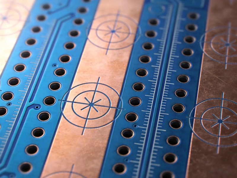
Before we get into assembly, it helps to know what came before it. Pcb fabrication is the process of making the bare circuit board itself—the fiberglass substrate, the copper layers etched into traces, the solder mask coating, and the silkscreen markings. Think of it like building the frame of a house: you have the structure, but nothing's inside yet.
Pcb Assembly is what comes next: taking that bare board and populating it with components. Resistors, capacitors, ICs, connectors—every part that makes the board actually do something gets placed and soldered during assembly. If fabrication is building the frame, assembly is everything that goes inside it—the plumbing, the wiring, the fixtures.
Most people who say they're looking for "Pcb assembly services" actually mean they need both fabrication and assembly together, which is why many manufacturers offer them as a combined one-stop service. But the processes are distinct, and understanding the difference matters when you're debugging problems or evaluating suppliers.
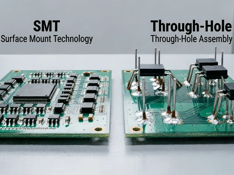
SMT is the dominant assembly method in use today, accounting for the vast majority of all Electronics Production. In surface mount, components are placed directly onto the surface of the board—no holes required. The component leads sit flat on solder pads, and Solder Paste—basically tiny spheres of solder mixed with flux—holds everything in place during reflow.
The advantages of SMT are substantial:
Through-hole was the original method and is still used where durability and mechanical strength matter most. In THT, component leads are inserted through holes drilled in the board and soldered on the opposite side. The solder joint is mechanically stronger than surface mount, which makes through-hole ideal for components that experience physical stress—connectors that get plugged and unplugged, parts subject to vibration, or components that carry high current.
The tradeoff: through-hole requires drilling holes (adding cost), limits component placement to one side of the board, and generally takes longer to assemble. But for the right applications, the mechanical robustness is worth it.
Most modern products use a combination of both methods—SMT for most components, through-hole for the parts that need it.
Here's how a board goes from a bare green panel to a finished, tested assembly. Every step matters, and quality at each stage compounds into the final result.
The process starts with your design data—Gerber files for the board, drill files, BOM (bill of materials), and pick-and-place files. Before any production, a good manufacturer runs a Design for Manufacturability (DFM) review to catch issues like component spacing that's too tight, pad sizes that don't match the actual parts, or routing that might cause problems during assembly. This step catches expensive mistakes before they're baked into production boards.
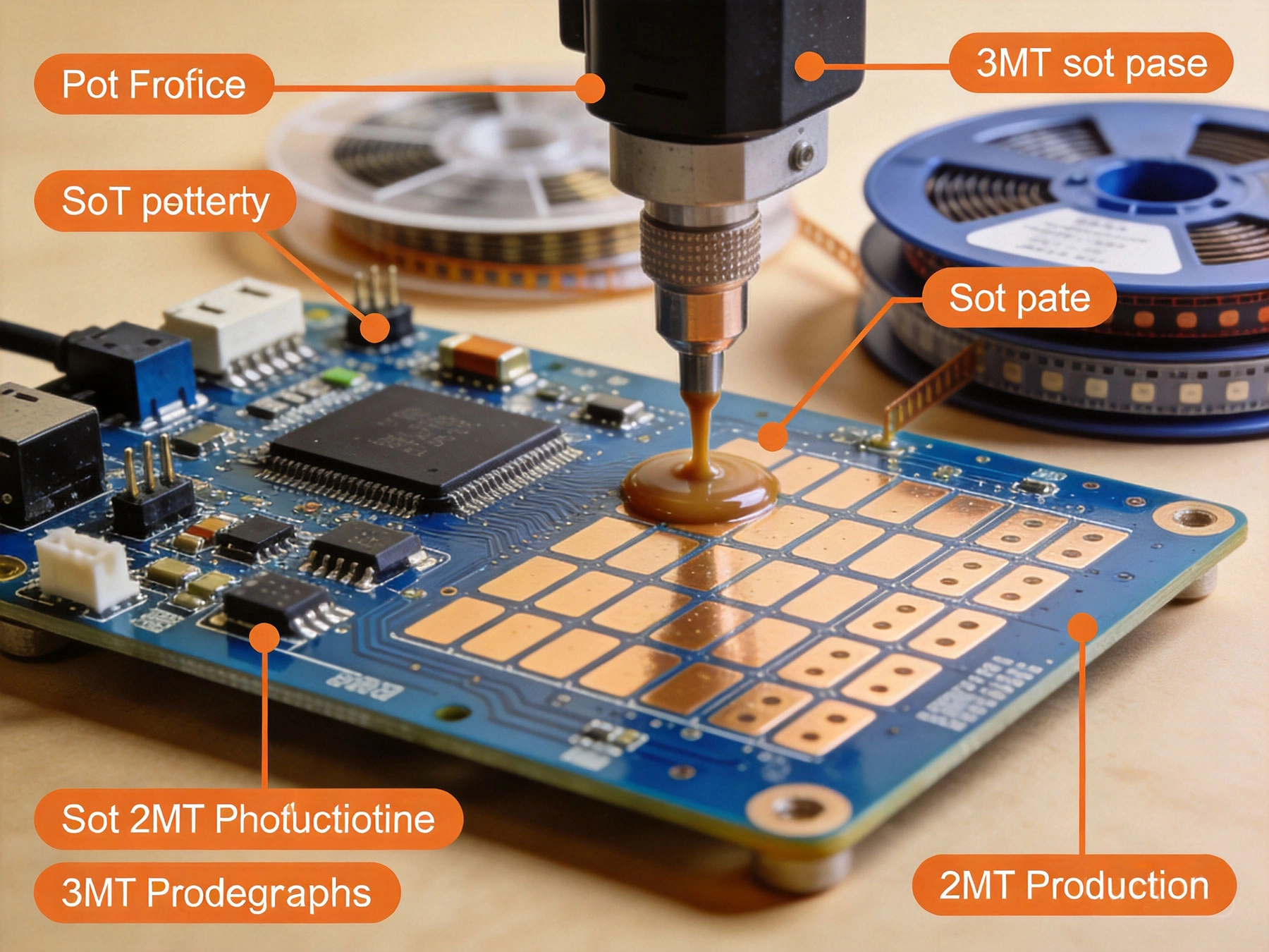
The bare PCB arrives from the fabrication stage and gets cleaned and inspected. Then Solder Paste—a mixture of fine solder particles and flux—is applied to the pads where surface mount components will go. This is done with a steel stencil cut to match exactly the pad pattern on your board. The paste is squeegeed across the stencil, filling the openings and depositing precise amounts on each pad. The accuracy here matters enormously: too much paste can cause bridges, too little can result in open joints.
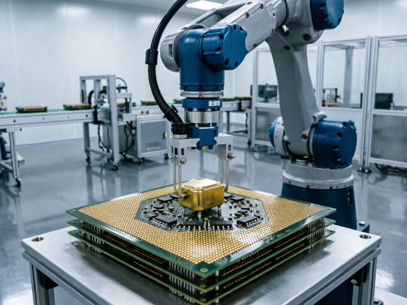
After paste printing, the board moves to the pick-and-place machine. Modern machines are remarkable pieces of engineering—vision systems recognize each component from above, vacuum nozzles pick parts from reels or trays, and placement heads position them with accuracies measured in microns. A typical high-speed SMT line can place 30,000 to 80,000 components per hour. The machine places each part on the still-wet solder paste, which holds it in position.
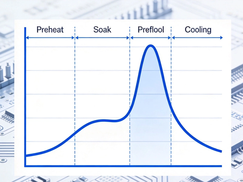
The board with all its components goes into a reflow oven—a long conveyor belt passing through carefully controlled heating and cooling zones. The oven follows a precise Temperature Profile: first warming gradually to activate the flux, then hitting the peak temperature where the solder paste melts and forms metallurgical bonds with the component leads and pads, then cooling to solidify the joints. Get the profile wrong and you get cold joints, Tombstoning, or components that have been damaged by excessive heat. The profile is typically tuned for each product, and it's one of the most critical parameters in Smt Assembly.
For boards using through-hole components, these are inserted after SMT reflow—either manually by technicians or automatically with radial/axial insertion machines. Through-hole parts are typically hand-soldered or wave-soldered, where the board passes over a wave of molten solder that wicks up into the holes by capillary action. Some mixed-technology boards go through both Wave Soldering and hand touch-up to complete through-hole connections.
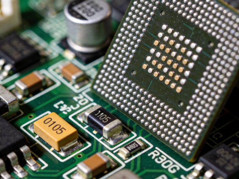
After soldering, every board gets inspected. AOI (Automated Optical Inspection) uses cameras and software to check for obvious defects—Missing Components, misaligned parts, solder bridges, insufficient solder. For boards with BGA or QFN packages where solder joints are hidden beneath the component, X-ray inspection is used to verify the hidden joints. Boards that fail inspection go to rework for correction. Some manufacturers also run in-circuit test (ICT) or flying probe testing to verify electrical connectivity.
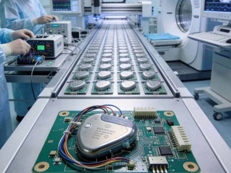
For boards with microcontrollers, FPGAs, or other programmable components, the firmware gets loaded at this stage. Then the board goes through functional testing—applying power, exercising the circuits, verifying that it behaves as designed. For a consumer product this might be a simple boot test; for medical or automotive boards it could be hours of rigorous validation. The depth of functional test depends on the product's reliability requirements and the manufacturer's quality system.
For boards that will operate in harsh environments—automotive under-hood applications, outdoor electronics, marine equipment—a Conformal Coating may be applied. This is a thin polymer film that coats the assembly and protects it from moisture, dust, and contaminants. After coating (if needed), the board goes through final inspection, cleaning, and packaging for shipment.
| Factor | Surface Mount (SMT) | Through-Hole (THT) |
|---|---|---|
| Component size | Very small (0201, 01005 passives, fine-pitch ICs) | Larger packages (resistors, caps, connectors) |
| Board real estate | Both sides usable | One side only |
| Mechanical strength | Moderate | High — ideal for connectors, high-stress parts |
| Assembly speed | Very fast — automated Pick And Place | Slower — drilling and manual insertion |
| Typical cost | Lower for high-volume production | Higher due to drilling and labor |
| Best for | Most modern electronics, miniaturized products | High-reliability, high-current, high-vibration apps |
| Repairability | Difficult for fine-pitch parts | Easier — joints are accessible |
Modern electronics are more demanding than ever. The components are smaller, the boards are denser, and the products they're in are expected to work reliably for years without service. A poorly assembled board doesn't just fail—it can damage brand reputation, trigger expensive field returns, and in some applications, create safety hazards.
What separates a quality PCBA partner from a marginal one isn't just equipment—it's the combination of engineering expertise, process discipline, and quality systems that catch problems before they ship. A manufacturer who runs DFM reviews, maintains calibrated equipment, uses statistical process control, and has documented inspection procedures will consistently outperform one who assembles boards by the cheapest method and hopes for the best.
"We learned the hard way that the cheapest assembly quote is almost never the cheapest solution. Our first PCBA vendor had great pricing but a 12% first-pass yield failure rate. After we switched to a manufacturer with proper AOI, X-ray inspection, and functional test, our field failure rate dropped by 97%. The difference in cost per good unit was night and day."
— Founder, Hardware Startup, Austin TX
If you're commissioning your first PCBA build—whether it's a prototype, a pilot run, or a production order—here's what to look for in a manufacturing partner:
Submitting files directly to production without a DFM review is like building a house without a building inspector. You might get lucky and find no issues, but if problems exist, you'll pay for them in rework, delays, and scrap. Always request a DFM review, even for prototypes. It's almost always free and almost always catches something worth fixing.
If you specify a component that's long-lead, obsolescent, or from a single source with limited availability, you're setting up for delays and price spikes. Always ask your assembler about component availability, and build in second-source options where possible.
The solder paste stencil is a low-cost item that has an outsized impact on assembly quality. A poorly made stencil—wrong thickness, poorly cut openings, damaged coating—causes a disproportionate number of assembly defects. Ask your manufacturer about their stencil process.
PCB assembly is not a commodity. A board from a state-of-the-art facility with AI-powered inspection and rigorous process control is categorically different from a board assembled in a low-cost shop cutting every corner. The price difference is real, but so is the quality difference—and for most products, the Total Cost Of Ownership strongly favors quality.
Understanding PCB assembly is just the beginning. Once you have a solid grasp of the basics, you'll naturally move into more advanced territory: DFM principles for specific architectures, embedded component design, high-speed signal layout, thermal management, and reliability engineering. Each of these areas builds on the foundation covered here.
If you're working on a hardware product, the best advice is to find a manufacturing partner early—ideally during the schematic design phase, certainly before layout—and treat them as a resource. The best EMS providers don't just execute your designs; they help you design things that can be built reliably and efficiently.
Whether you're building your first prototype or scaling a product to volume, understanding the PCB assembly process gives you a significant advantage. You're better equipped to design for manufacturability, evaluate manufacturing partners, and make informed decisions at every stage of your product's journey. The foundation is here—now it's time to put it to work.
For a standard multilayer board with standard surface finishes, typical lead time ranges from 10 to 15 business days from order confirmation to ship date. Complex boards—high layer counts, advanced packages, impedance-controlled RF designs—can take 15 to 25 business days. Expedited service is usually available for a premium. The longest lead times usually come from Component Procurement for parts that aren't in stock, so building a relationship with a manufacturer who has distributor relationships and can expedite procurement is worth the effort.
It varies significantly by manufacturer. Some shops specialize in prototype and low-volume work and will build as few as 5 to 10 boards. Others have minimum order quantities (MOQs) of 50, 100, or more. If you need fewer boards than a shop's MOQ, look for providers with dedicated prototype or NPI services.
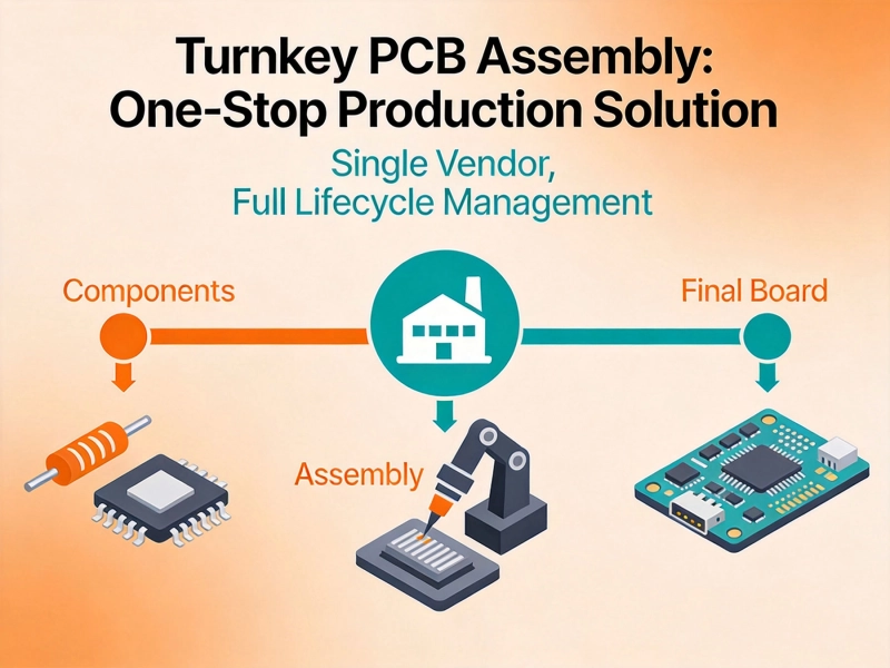
Yes, most PCBA manufacturers accept customer-supplied components. This is called "consigned" or "CEM" (Contract Electronics Manufacturer) assembly. The trade-off is that you're responsible for component quality, availability, and any costs if parts arrive damaged or incorrect. Full Turnkey Assembly—where the manufacturer sources everything—is often more convenient and can actually be cheaper when they have established distributor relationships and volume pricing.
Defective boards go to a rework station where technicians diagnose and repair the specific issue—replacing a bad component, reflowing a cold joint, fixing a bridge. After rework, the board runs through inspection again. A quality manufacturer will provide a defect report showing what failed and why, and should work with you to prevent recurrence in subsequent builds.
These terms overlap significantly and are often used interchangeably. EMS stands for Electronics Manufacturing Services—the broadest term covering design, assembly, test, and sometimes logistics. CEM (Contract Electronics Manufacturer) is similar, often emphasizing manufacturing-only rather than design services. PCBA specifically refers to the assembly process itself. In practice, when you're looking for someone to build your boards, all three terms usually mean the same thing.
What is the difference between Surface Mount Technology (SMT) and through-hole assembly?June/04/2026
What is Reflow Soldering and Why Does the Temperature Profile Matter?July/14/2026
Why Choose Turnkey PCB Assembly for Your Next Product Launch?May/22/2026
Fiducial Marks and Tooling Holes: Ensuring Precision in SMT PlacementJuly/15/2026
Why High-Reliability PCB Assembly is Critical for Medical DevicesJune/02/2026
How Turnkey Providers Streamline Component Procurement and LogisticsJune/18/2026
Miniaturization Mastery: Handling 01005 Components and Micro BGAsJune/15/2026
Understanding the True Cost Drivers in Modern Electronics ManufacturingJuly/20/2026