Open Nav


From mastering Design for Manufacturability (DFM) rules to optimizing pad layouts and thermal relief, our articles provide actionable technical guidance to prevent defects and enhance product reliability for engineers and designers.
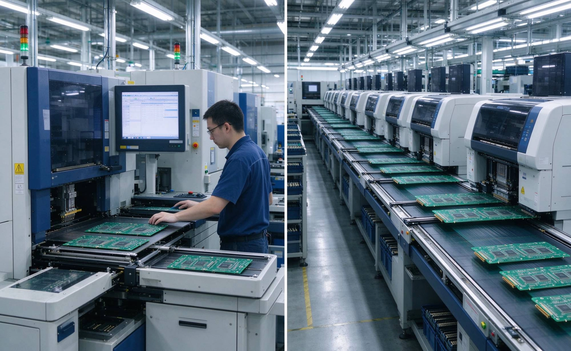
The Difference Between Quick Turn PCB Assembly and Standard ProductionWhen hardware development teams need circuit boards assembled, the choice between quick turn assembly and standard production is rarely straightforward. Both approaches produce functional, reliable assemblies, but they serve fundamentally different purposes in the product development lifecycle. Ma...

Understanding Prototype SMT Assembly China: A Step-by-Step GuideGetting prototype boards assembled in China is one of the most efficient ways to move from design to hardware — but only if you understand the process and prepare properly. The SMT assembly line is a sophisticated, high-speed system that expects consistent, well-formatted inputs. When your files, ...
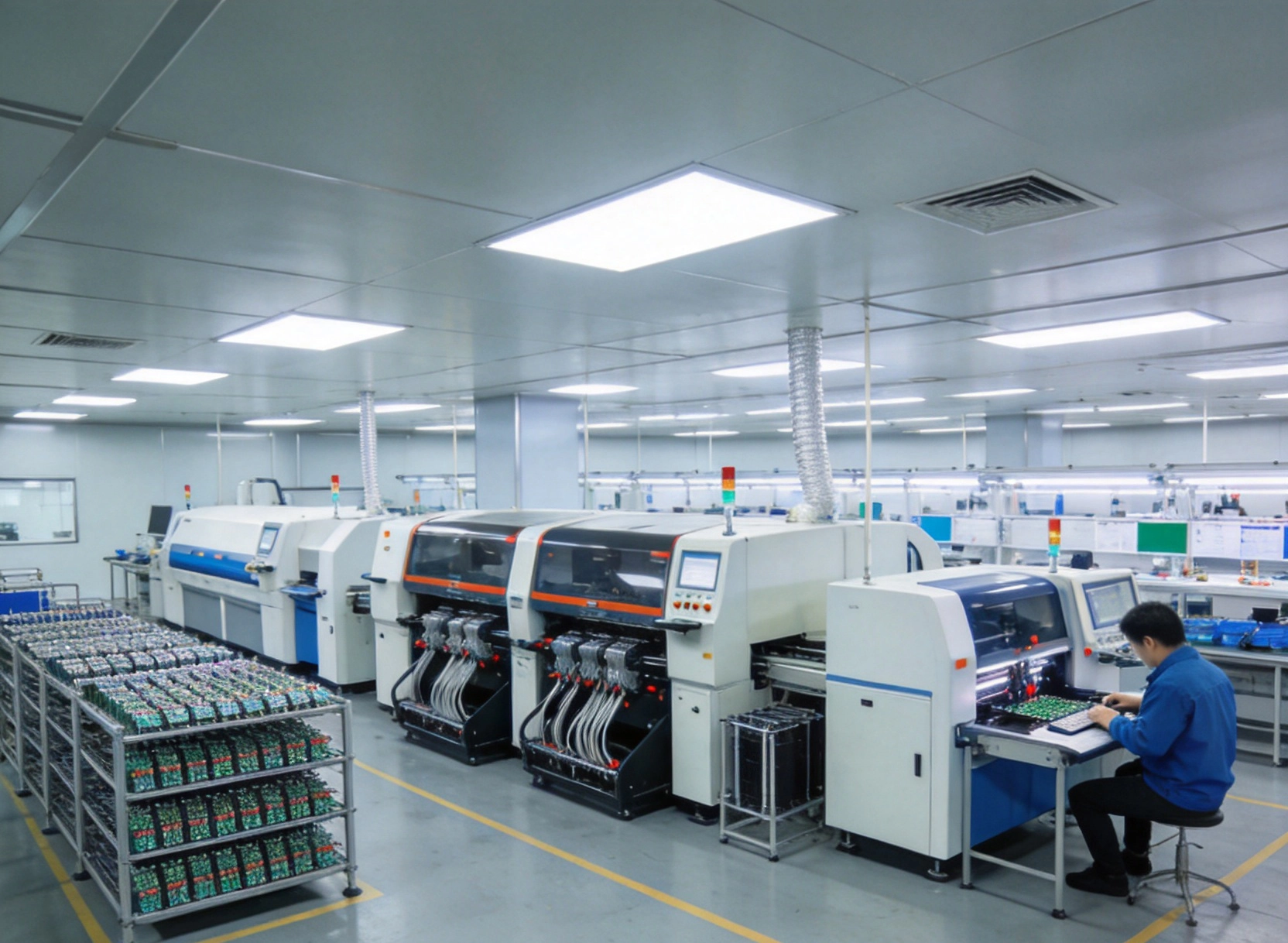
What is Turnkey PCB Assembly? A Beginner's GuideIf you have ever needed printed circuit boards assembled with components, you have likely encountered the term "turnkey PCB assembly." This service model has transformed how companies bring electronic products from concept to reality. Yet for those new to electronics manufacturing, understanding w...
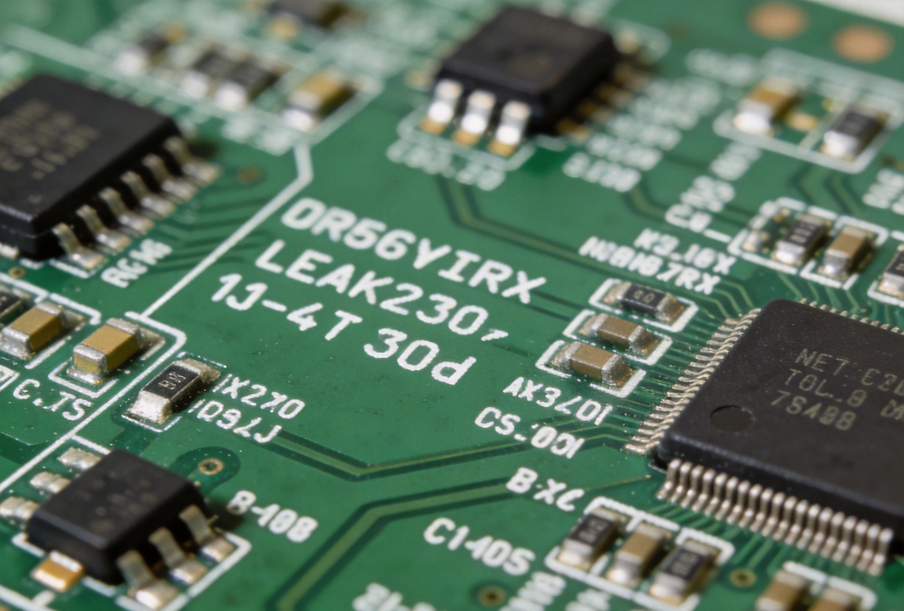
Silk Screen Best Practices: Improving Readability and Assembly EfficiencySilkscreen markings on printed circuit boards often get treated as an afterthought—something to add after trace routing is complete. This attitude creates problems that ripple through manufacturing, testing, and field service. When assembly technicians struggle to identify components, or when docu...
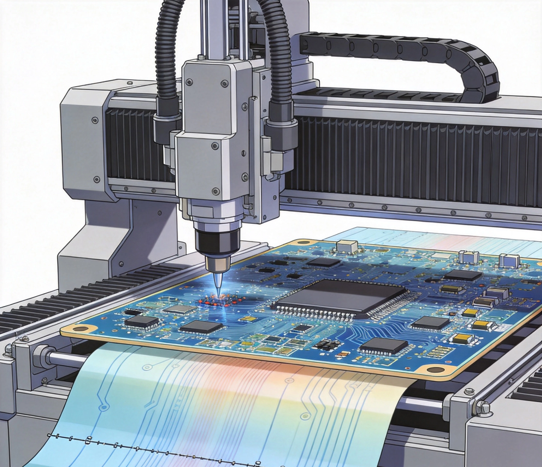
Solving Assembly Stress Issues in Large and Thin PCBsLarge and thin PCBs present unique manufacturing challenges that can compromise product quality and yield if not properly addressed. The physics of thin boards with substantial surface area creates susceptibility to warpage, handling damage, and assembly-induced stress that thicker boards handle w...
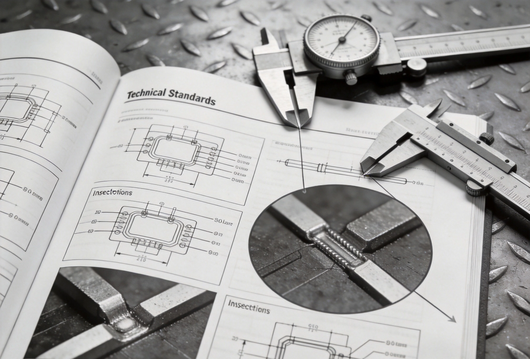
How to Read an IPC-A-610 Standard for Electronic AssembliesThe IPC-A-610 standard is the most widely referenced inspection standard in the electronics assembly industry. Officially titled "Acceptability of Electronic Assemblies," it defines the visual acceptance criteria for electronic components mounted on printed circuit boards, covering everything from...

China's Role in the Global PCB Assembly Ecosystem: A 2026 UpdateFor most of the past three decades, the sentence "the world's electronics are built in China" has been so consistently true as to feel almost unremarkable. But the global PCB assembly ecosystem in 2026 is more dynamic and contested than at any point in that history. Supply chain disruptions, geopo...
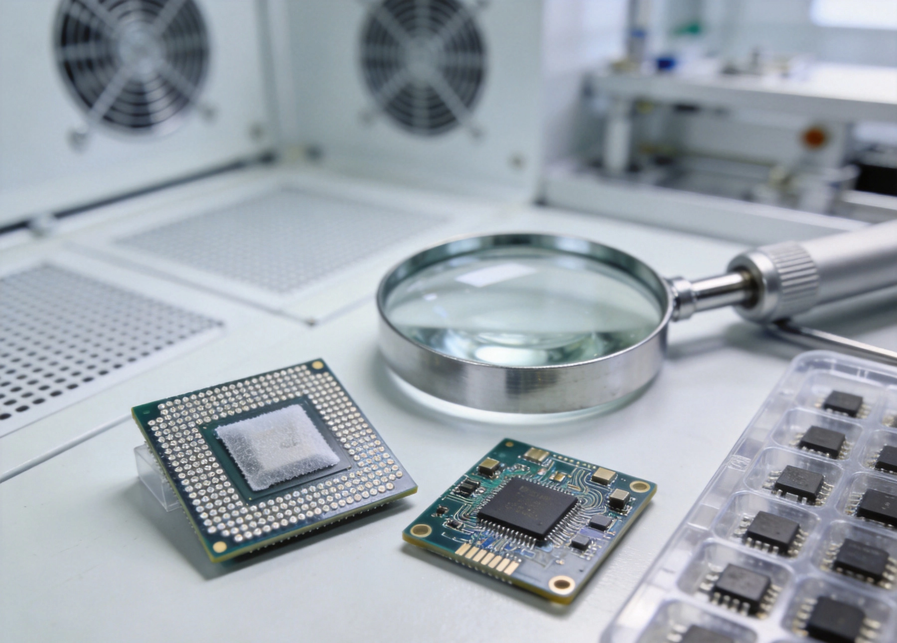
Managing Moisture Sensitivity Levels (MSL) for BGA and QFN PackagesMoisture inside electronic packages creates serious reliability risks during surface mount assembly. When moisture-sensitive components absorb humidity from the environment and then encounter rapid heating during reflow soldering, the resulting steam pressure can crack package bodies, delaminate i...
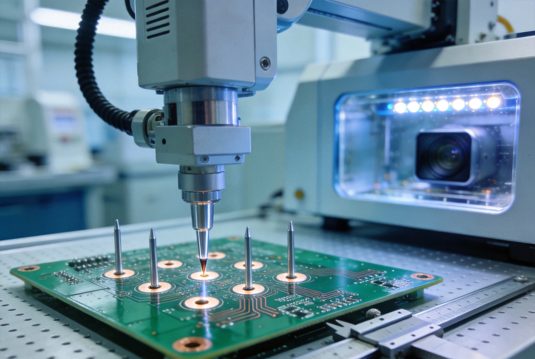
Designing for Testability (DFT): Placing Test Points for ICT and FCTManufacturing electronic assemblies without comprehensive testing invites costly field failures and customer returns. Yet testing effectiveness depends heavily on design decisions made long before production begins. Designing for testability, commonly abbreviated as DFT, ensures that PCBs can be t...

Thermal Relief Design: Balancing Heat Dissipation and SolderabilityIn PCB design, thermal relief is one of those topics that seems obscure until a board comes back from assembly with cold solder joints, lifted pads, or — paradoxically — traces that burned out under load. The thermal relief pattern surrounding a pad or via is the interface between the component, t...
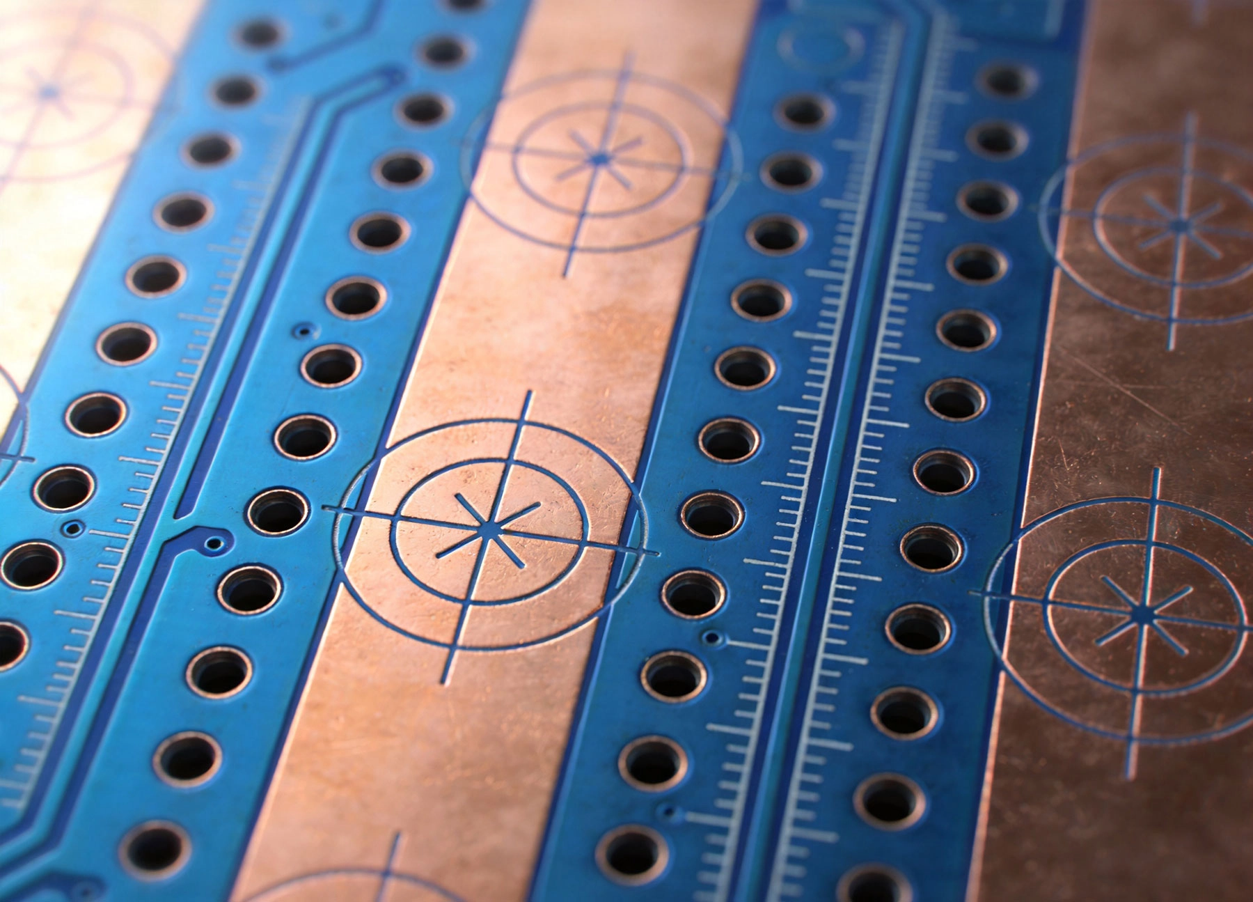
Fiducial Marks and Tooling Holes: Ensuring Precision in SMT PlacementEvery millimeter counts in surface mount technology assembly. As component packages shrink from 0402 to 0201 to 008004, the tolerance for placement error narrows to fractions of a millimeter. Miss by too much, and solder joints fail. Align poorly on fine-pitch parts, and bridging destroys expensiv...
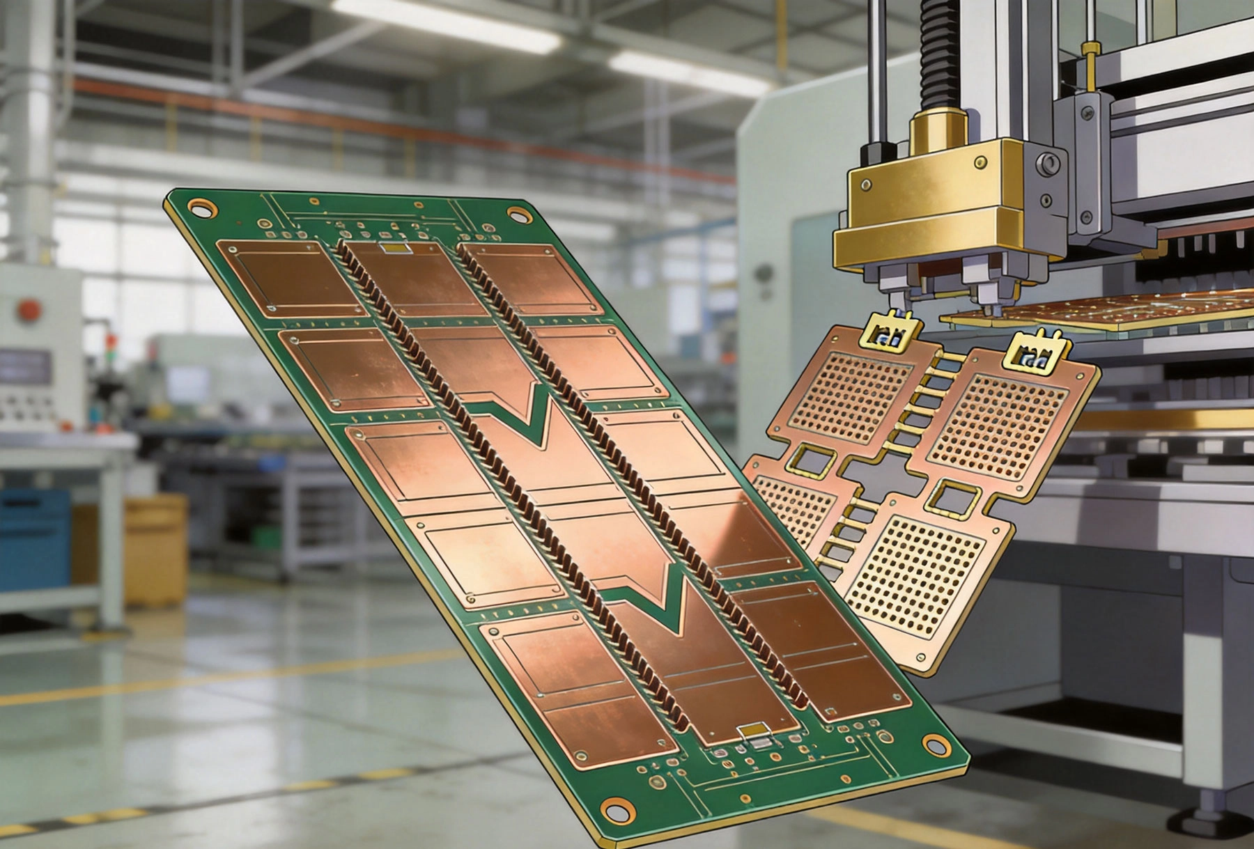
Panelization Strategies: V-Scoring vs. Tab Routing for Efficient DepanelingEvery printed circuit board begins its manufacturing life as part of a larger panel—a rectangular array of identical boards joined together before being separated into individual units. This panelization strategy, invisible to most PCB buyers, profoundly affects manufacturing efficiency, assembly ...
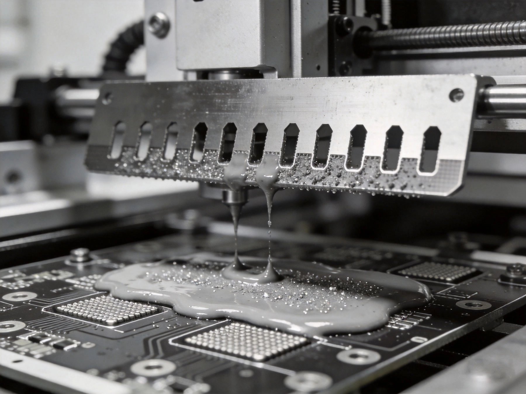
The Science of Solder Paste Printing: Stencil Design Best PracticesIn the world of surface mount technology (SMT) assembly, solder paste printing stands as the most critical—and often most problematic—process step. Studies consistently show that 50-70% of all SMT defects originate from poor solder paste printing. Yet despite its importance, stencil design is freq...
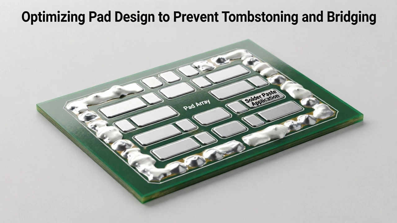
Optimizing Pad Design to Prevent Tombstoning and BridgingIf you have ever spent hours debugging a prototype only to find out that your tiny 0201 resistors are standing straight up like little tombstones, you know the pain. Surface Mount Technology (SMT) is amazing, but it is unforgiving. Optimizing pad design to prevent tombstoning and bridging is one o...
Mastering DFM: Essential Design Rules for Flawless PCB AssemblyThe design decisions that determine whether your board assembles perfectly—or costs you weeks and thousands in reworkHere's a number that should make every hardware engineer wince: industry data consistently shows that 40% to 60% of all PCB assembly defects trace directly back to design de...