

Getting prototype boards assembled in China is one of the most efficient ways to move from design to hardware — but only if you understand the process and prepare properly. The Smt Assembly line is a sophisticated, high-speed system that expects consistent, well-formatted inputs. When your files, components, or specifications have gaps, the result is delays, errors, and boards that do not work. This guide walks through every step of prototype Smt Assembly at a Chinese manufacturer, from the files you submit to the finished boards you receive, so you know exactly what happens at each stage and what you need to provide.

Everything starts with the data you send. A complete and accurate file package is the single most important factor in a smooth prototype build. Missing or inconsistent information is the number one cause of delays.
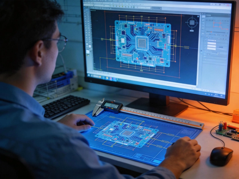
Before any Manufacturing begins, the assembler reviews your design for manufacturability and validates the BOM. This step catches issues that would cause failures on the line.
The assembler checks every BOM line item for availability, MOQ, and lead time. For prototype builds, this is particularly important because:
At this stage, the assembler will flag any issues and propose resolutions — alternative parts, design modifications, or schedule adjustments. You must approve these before the build proceeds.
For turnkey prototype builds, the assembler purchases all BOM components. For consignment builds, you ship components to the assembler. In either case, incoming inspection is critical.
Chinese assemblers typically source components from a combination of franchised distributors (for mainstream parts), authorized agents (for Asian-sourced ICs), and spot-market brokers (for hard-to-find parts). For prototypes, the assembler may use distributors that support small-quantity purchases — cut-tape, partial reels, and loose-piece options that avoid full-reel MOQs.
The assembler will prioritize purchasing from franchised sources to minimize counterfeit risk. If any component must be sourced from the open market, they should inform you and provide traceability documentation.
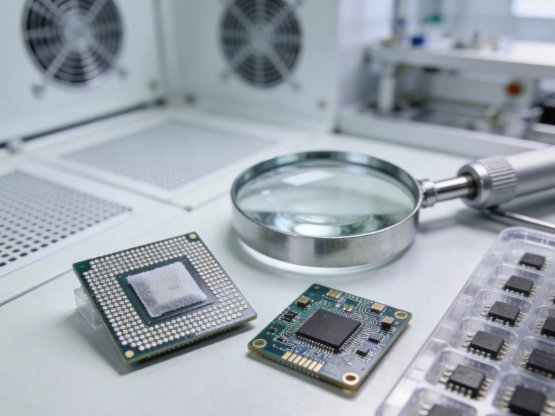
Many SMT components — especially QFPs, BGAs, and chip-scale packages — are moisture-sensitive. When exposed to ambient humidity, they absorb moisture that can vaporize explosively during reflow (the "popcorn" effect). Components are rated by Moisture Sensitivity Level (Msl), which defines the maximum floor life before baking is required.
At a Chinese prototype assembler, MSDs are stored in moisture-barrier bags with desiccant and humidity indicator cards. Before assembly, the assembler checks the exposure time against the Msl rating. If the floor life has been exceeded, the components are baked at 125°C for the required time (typically 8-24 hours depending on the MSL level and package thickness).
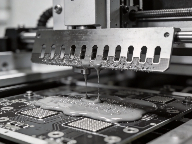
The solder paste stencil is a thin metal sheet (typically stainless steel) with apertures that correspond to the solder paste pads on your board. The stencil controls how much solder paste is deposited on each pad — too much causes bridging, too little causes insufficient solder and weak joints.
For prototype builds, the stencil is typically laser-cut from stainless steel foil. Laser cutting is fast (1-2 day turnaround) and produces clean, accurate apertures. Electroformed stencils offer smoother aperture walls but are more expensive and slower to produce, making them more appropriate for production.
Solder Paste Printing is the most process-critical step in SMT assembly. Studies consistently show that 60-70 percent of SMT defects originate at the printing stage. Getting the paste deposit right — correct volume, position, and shape on every pad — is the foundation of a successful build.
For prototype builds, many Chinese assemblers perform 100 percent Solder Paste Inspection using 3D SPI equipment. SPI measures the volume, height, area, and shape of every paste deposit and flags deposits that are outside specification. This catches printing defects before components are placed, when correction is simple and inexpensive — just clean the board and reprint. Without SPI, printing defects are not detected until after reflow, when rework is much more difficult and time-consuming.
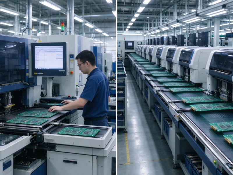
The pick-and-place machine is the heart of the SMT line. Modern high-speed placers can position 30,000-100,000 components per hour with placement accuracy of ±25-50 µm. For prototype builds, speed is less important than accuracy and flexibility — the machine must handle the specific mix of component packages on your board.
Reflow Soldering melts the solder paste, creating permanent metallurgical connections between component terminations and PCB pads. The reflow profile — the temperature curve the board follows as it passes through the oven — must be carefully controlled to ensure reliable solder joints without damaging components.
A standard lead-free reflow profile has four zones:
For prototype builds, the assembler typically runs a thermal profile test using a profile board with thermocouples attached to representative component locations before running the actual build. This test verifies that all locations on the board reach the required peak temperature and TAL without exceeding the maximum temperature rating of any component. For boards with large thermal mass variations (a big transformer next to tiny 0402 resistors), the profile may need careful optimization to avoid overheating small components while ensuring the large component's joints fully reflow.
After reflow, the boards are inspected for solder joint quality and component placement accuracy. For prototypes, inspection is typically more thorough than for production because the design itself is being validated.
AOI uses high-resolution cameras and image processing algorithms to inspect solder joints and component placement. It detects:
For prototypes, AOI is typically run at a more sensitive threshold than production, catching marginal defects that might be waived in volume production. This is appropriate because the goal of prototype inspection is to identify design-related defects (land pattern issues, paste volume problems) that need correction before production.
For boards with Bga, Qfn, or LGA components, X-ray inspection is essential because the solder joints are hidden under the component body and cannot be seen by optical inspection. X-ray reveals:
Chinese prototype assemblers typically perform X-ray inspection on all BGA components, especially for first articles. Some facilities use 2D X-ray, while others have 3D CT (computed tomography) capability for more detailed analysis.
Even with AOI and X-ray, manual inspection by a trained operator is standard for prototype builds. The operator checks for issues that automated systems may miss — scratched components, bent leads on through-hole parts, proper orientation of polarized components, and general workmanship quality.
If your board has through-hole components — connectors, large capacitors, power devices — they are assembled after SMT reflow. The method depends on the component mix:
After soldering, flux residue remains on the board surface. Whether cleaning is required depends on the flux type:
Conformal Coating is a protective dielectric layer applied over the assembled board to protect against moisture, dust, chemical exposure, and mechanical abrasion. For prototypes, Conformal Coating is typically not applied unless the application requires it (outdoor use, high humidity, high voltage). If required, the coating is applied by spray, dip, or selective coating robot, then cured by UV, thermal, or moisture-activated mechanisms.
Electrical testing verifies that the assembled board functions correctly. The testing approach depends on the board complexity and your requirements:
ICT uses a bed-of-nails fixture to access individual nets and test components in isolation. It verifies component values, checks for opens and shorts, and tests basic functionality of individual devices. For prototypes, ICT is used when the design has test points that allow probe access. The fixture cost makes ICT more practical for production, but some prototype assemblers offer flying probe testing as a fixture-less alternative.
Functional testing powers the board and verifies that it operates as intended in its normal configuration. This is the most meaningful test for prototypes because it validates the complete design — not just individual component values but the system-level interaction of all parts. Functional test procedures are typically defined by you (the customer) and may involve connecting the board to test equipment, running firmware, and verifying outputs.
Flying probe testing uses moving probe heads to access test points without a fixture. It is ideal for prototypes because it requires no tooling cost and can test any board with accessible nets. The trade-off is speed — flying probe is much slower than ICT (minutes per board versus seconds), but for prototype quantities this is not a concern.
The final step is getting your boards to you safely. Chinese assemblers typically offer several shipping options for prototype orders:
Boards are packaged in ESD-safe materials — anti-static bags, bubble wrap, and rigid cardboard boxes. Moisture-sensitive boards may be sealed in moisture-barrier bags with desiccant for ocean shipments.
Understanding the typical timeline helps you plan your project schedule. Here is a realistic timeline for a standard prototype SMT build at a Chinese assembler:
Total elapsed time from file submission to boards in hand is typically 2-3 weeks for a standard prototype with readily available components. Builds with long-lead components may take 4-6 weeks.
Most Chinese assemblers accept prototype orders as small as 5-10 boards. Some specialize in very small runs (1-5 pieces) for early-stage startups. The per-board cost is higher for small quantities because setup costs (stencil, programming, first-article inspection) are amortized over fewer units, but the absolute cost is low and the turnaround is fast.
Yes. Consignment Assembly is supported by most Chinese assemblers. You ship your components to them, and they handle the assembly. Be aware that you bear responsibility for component quality and completeness — if any part is missing, incorrect, or damaged in shipping, the build will be delayed. For prototypes where you have specialized or hard-to-source components, consignment makes sense. For everything else, turnkey is usually simpler and faster.
For turnkey builds, the assembler should never substitute a component without your written approval. If a BOM part is unavailable, the assembler will propose alternatives (typically same-function, same-package parts from different manufacturers) and wait for your approval before proceeding. For passives (resistors, capacitors), cross-referencing is straightforward. For ICs, substitutions require more careful evaluation of electrical compatibility.
If the assembler discovers a design error during Dfm Review — before Manufacturing — they will flag it and you can correct the design. If an error is discovered after assembly (e.g., a wrong component value that passes Visual Inspection but causes functional failure), the assembler will report the finding. You can then decide whether to have the boards reworked (if the error is correctable) or to redesign and rebuild. Most prototype assemblers include first-article review precisely to catch these issues early.
Not typically. Modern Chinese SMT assemblers provide detailed documentation — photos, inspection reports, X-ray images, and test results — that give you visibility into the process without being on-site. For first-time builds with a new supplier, some customers visit for a process audit, but for routine prototype orders, remote communication and documentation are sufficient.
Understanding the complete SMT assembly process — from file preparation through final testing — is the key to successful prototype builds in China. Each step has specific requirements and failure modes, and your preparation at each stage directly impacts the quality and speed of the build. Submit complete and consistent files, review DFM feedback carefully, approve BOM and procurement decisions promptly, and specify your testing requirements clearly. When you understand what happens at each step, you can anticipate problems, provide the right information, and work with your assembler as a partner rather than just a customer. The result: prototype boards that work the first time, delivered on schedule, at a price that keeps your project moving forward.
Contact us to discuss your requirements
Managing Moisture Sensitivity Levels (MSL) for BGA and QFN PackagesAugust/10/2026
Mastering DFM: Essential Design Rules for Flawless PCB AssemblyMay/22/2026

Thermal Relief Design: Balancing Heat Dissipation and SolderabilityJuly/23/2026
Fiducial Marks and Tooling Holes: Ensuring Precision in SMT PlacementJuly/15/2026
What is Turnkey PCB Assembly? A Beginner's GuideSeptember/23/2026
The Difference Between Quick Turn PCB Assembly and Standard ProductionOctober/16/2026
The Science of Solder Paste Printing: Stencil Design Best PracticesJune/17/2026
Panelization Strategies: V-Scoring vs. Tab Routing for Efficient DepanelingJuly/07/2026