Open Nav


Here's a number that should make every hardware engineer wince: industry data consistently shows that 40% to 60% of all Pcb Assembly defects trace directly back to design decisions—not Manufacturing errors, not component quality issues, not machine calibration drift, but choices made at the schematic and layout stage. Every one of those defects started as a decision that seemed fine in CAD but created a Manufacturing problem that no amount of process control could fully compensate for. Design for Manufacturability—DFM—exists to close that gap between design intent and producible reality. This guide gives you the essential rules that every Pcb designer needs to internalize before sending files to manufacturing.
DFM gets talked about like it's an optional nice-to-have, something you do if you have time left over after the "real" design work. That's backwards. DFM is foundational. It starts at schematic design—component selection, architecture decisions, the fundamental approach—and it continues through every stage of layout until your files are released for manufacturing.
The goal of DFM isn't to make your design conform to arbitrary manufacturing limitations. It's to identify the intersection between your electrical requirements, your product's use case, and the practical capabilities of the assembly processes available to you. A well-DFM'd board isn't dumbed down—it's optimized to be built reliably, at target cost, in the quantities you need.
The best engineering teams treat their manufacturing partner as a DFM resource, not just a production vendor. They engage during design, share their requirements, and incorporate manufacturability feedback before the design is finalized. The result is boards that come back from assembly right the first time, with high first-pass yield and no surprises.
Component placement is where most DFM problems originate. Engineers who are thinking about routing often neglect the physical realities of how components actually get placed and soldered on a production line. The result: boards that look fine in CAD but can't be assembled reliably.
The minimum spacing rules that matter most:
| Parameter | Standard Assembly | High-Density / Fine-Pitch |
|---|---|---|
| Between SMT components (body-to-body) | 0.5mm minimum | 0.3mm (verify with manufacturer) |
| Component to board edge | 3.0mm minimum | 2.0mm (confirm with fab) |
| Component to Tooling Holes | 3.0mm minimum | 3.0mm |
| Between QFP/TQFP pins | 0.5mm pitch standard | 0.4mm pitch available |
| BGA to nearest component | 5.0mm minimum | 4.0mm minimum |
Orientation matters. All components of the same type should be oriented consistently—preferably in the same direction. This matters most for passives (resistors, capacitors) where rotated 0402s and 0201s look almost identical to the pick-and-place machine, but incorrect orientation on polarized components (LEDs, tantalum capacitors, electrolytic caps) causes immediate failure. Consistent orientation also dramatically improves AOI inspection accuracy.
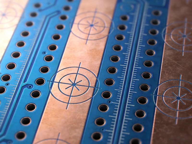
Keep fiducials clear. If your design uses board-level Fiducial Marks for placement accuracy, make sure there's at least 3mm of clear space around each fiducial—no traces, no silkscreen, no components within that radius. Fiducials placed too close to other features cause vision system confusion and reduced placement accuracy.
Maintain consistent component orientation for all passive devices. Place high components (connectors, tall caps) away from small components to avoid shadowing during reflow.
Placing components at irregular angles (45°, etc.) just to save routing space. It complicates paste printing, AOI inspection, and hand repair.
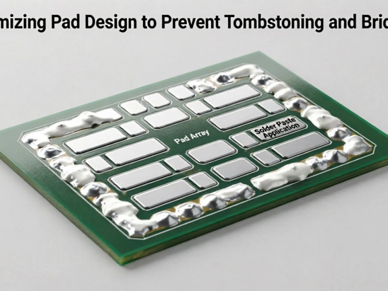
The pads on your Pcb—the copper shapes where components get soldered—are where electrical performance meets manufacturing capability. Get them wrong and you get opens, bridges, Tombstoning, or unreliable joints that fail in the field.
Key Pad Design principles:
Tombstoning—where a passive component lifts off one end and stands up like a tombstone—is almost always a DFM issue, not a process issue. It happens when the two Solder Paste deposits on either side of a component reflow at different rates, pulling the component toward the side that solidified first. The root causes are almost always pad size imbalance, uneven paste volume, or component landing patterns that don't match the datasheet. Fix the Pad Design and tombstoning goes away.
Trace routing is usually where engineers spend the most time in layout—but it's also where DFM often gets ignored in favor of electrical performance. Here's how to route in a way that supports both.
Trace width and current-carrying capacity:
| Trace Width | 1 oz Copper — External Layer | 1 oz Copper — Internal Layer |
|---|---|---|
| 0.254mm (10mil) | ~1A (limited by temperature rise) | ~0.7A |
| 0.508mm (20mil) | ~2A | ~1.4A |
| 1.016mm (40mil) | ~3.5A | ~2.5A |
Beyond basic current capacity, routing rules that affect manufacturing include:
Vias are one of the most common sources of DFM problems. They're easy to add in CAD, but each via has manufacturing implications: drill cost, plating complexity, signal integrity impact, and reliability under thermal cycling. Smart via strategy is a hallmark of well-designed boards.
Via sizing fundamentals:
Via types and when to use each:
Use via-in-pad for BGA escape routing when necessary—this routes directly through the BGA pad, simplifying routing. Make sure your manufacturer supports it, as it requires copper-filled or plugged vias to prevent solder wicking down the barrel.
Using dozens of small micro-vias on high-current traces. Small vias can't carry high current reliably. Use larger through-hole vias or multiple parallel vias for power delivery paths.
These three elements are often treated as cosmetic afterthoughts, but they have significant impact on assembly quality and board reliability.
Solder mask:
Silkscreen:
Surface finish:
| Finish Type | Characteristics | Best For |
|---|---|---|
| ENIG | Flat surface, good for fine-pitch BGAs, excellent shelf life | Fine-pitch components, RF boards, multiple assembly cycles |
| HASL | Inexpensive, variable surface coplanarity | Standard through-hole and large-pitch SMT, budget builds |
| Lead-Free HASL | RoHS compliant HASL, slightly rougher surface | RoHS compliance required, larger components |
| OSP | Very flat, thin coating, single assembly cycle | Fine-pitch SMT, fast-turn prototypes |
PCBs aren't manufactured as individual boards—they're fabricated in panels, typically 18" × 24" or 21" × 24". How your boards are organized on the panel has significant impact on manufacturing yield, assembly efficiency, and cost.
Panelization options:
Critical panelization rules:
Boards that can't be tested reliably are boards with unknown quality. Designing adequate test access into your board from the start is one of the highest-value DFM decisions you'll make.
Test point design fundamentals:
"We implemented a rule in our design process: no board gets released for fab without a completed DFM checklist reviewed by a second engineer. Our first-pass yield went from 73% to 96% within six months. The two-engineer review requirement only adds half a day to the schedule, but it catches things that a single person working at 10pm misses. It's the highest-leverage process change we made in three years of hardware development."
— Hardware Engineering Manager, Commercial Drone Company, Shenzhen
RF boards demand tight impedance control (±5% or tighter), requiring close collaboration with your fab on dielectric constant consistency, trace geometry control, and laminate material selection. Rogers and other high-frequency laminates must be specified with precise thickness tolerances. Grounding vias must be placed close to RF traces to minimize parasitic inductance.
Automotive Electronics must meet AEC-Q100, AEC-Q101, and AEC-Q200 component qualification requirements. Board-level requirements include expanded temperature range testing, thermal cycling validation, and specific design rules around solder joint reliability. IPC Class 3 requirements are typical.
Military and aerospace boards require full MIL-SPEC compliance in materials, processes, and documentation. This includes specific laminate material certifications, plated-through-hole Reliability Testing, and extensive documentation. These boards cost significantly more and have longer lead times, but the requirements are non-negotiable.
The most successful hardware teams don't just run through a DFM checklist before releasing files—they've internalized the manufacturability perspective so deeply that it informs design decisions from the first schematic. They think about test access while selecting components, about routing constraints while choosing the stack-up, about panel efficiency while organizing the layout. DFM becomes part of the design process, not an afterthought attached to it.
This mindset shift takes time, but it pays compounding returns. Boards that assemble cleanly the first time get to market faster, cost less to produce, and have fewer field failures. The engineers who build this habit deliver more reliable products with less stress and fewer late-night firefighting sessions. That's a pretty good return on investment for internalizing a few design rules.
DFM mastery separates engineers who consistently hit their market windows from those who spend months chasing yield problems. Apply these rules from the start of your next design, engage your manufacturing partner early, and build DFM as a core discipline into your hardware development process. The boards that come back from assembly with high first-pass yield—and the products that ship on time as a result—are the best evidence that DFM works.
DFM should start at component selection—before any layout begins. Choosing components that are available, properly packaged, and come with verified land patterns is the first DFM decision. Stack-up selection, layer count decisions, and routing constraints should all be informed by DFM considerations before layout begins. A proper DFM review of the layout files before release is the final gate. If you're only reviewing DFM after layout is complete, you're probably catching problems too late to fix them without significant rework.
IPC-6012 defines three classes of manufacturing quality: Class 1 (general electronics), Class 2 (dedicated service electronics), and Class 3 (high-performance/Harsh Environment Electronics). The classes define acceptable defect levels, conductor width tolerances, annular ring requirements, and other manufacturing parameters. Class 3 has the tightest tolerances and lowest defect allowances. Most commercial electronics target Class 2. Automotive, medical, and aerospace typically require Class 3. Know which class your product requires and specify it clearly to your manufacturer.
Components from different manufacturers using the same package type can have slightly different land pattern recommendations. When you have mixed manufacturers, design to the smallest recommended pattern (or the most conservative recommendation) that accommodates all the parts you're considering. This gives the most margin for reliable assembly.
Yes—significantly. Flex boards introduce bend radius requirements, minimum bend radius design rules, different material stack-up considerations, and unique depanelization challenges. Stiffener attachment, coverlay design, and pad flexibility for dynamic flex applications all require specialized DFM knowledge. If you're designing flex or rigid-flex, work with a manufacturer who has specific flex expertise.
Probably not designing test access from the beginning. Engineers focused on routing and component placement often leave test point design to the end—and then find that critical nets are buried under BGAs with no accessible probe point, or that all the test points ended up on the bottom side because there wasn't room on the top. Designing test access in from the beginning—treating test points as a first-class design requirement, not an afterthought—eliminates this problem entirely.
Panelization Strategies: V-Scoring vs. Tab Routing for Efficient DepanelingJuly/07/2026
Fiducial Marks and Tooling Holes: Ensuring Precision in SMT PlacementJuly/15/2026
Optimizing Pad Design to Prevent Tombstoning and BridgingJune/05/2026
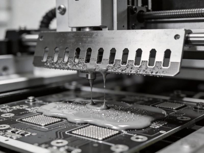
The Science of Solder Paste Printing: Stencil Design Best PracticesJune/17/2026
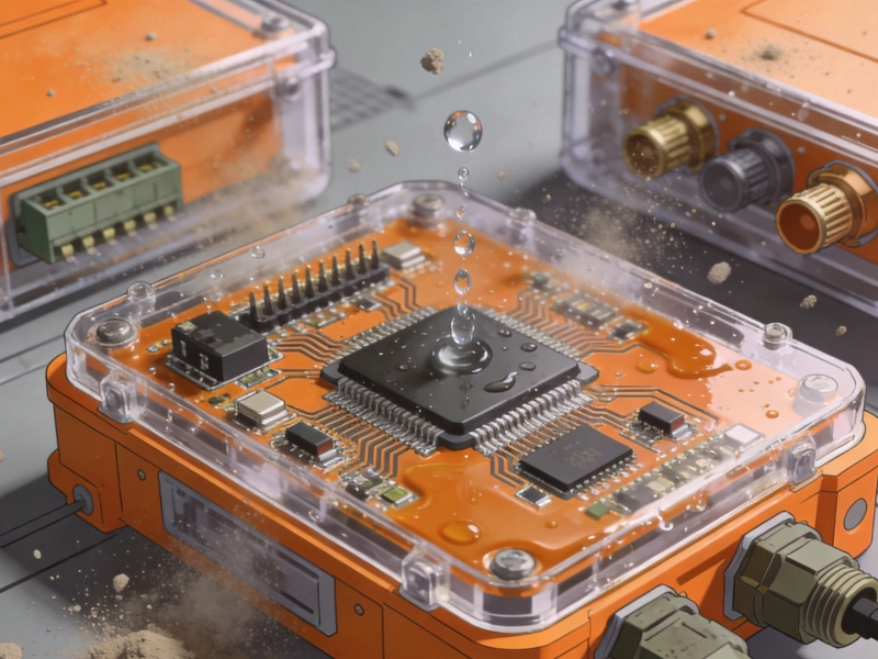
Specialized Assembly Solutions for Harsh Environment ElectronicsJuly/18/2026

Top 5 PCB Assembly Trends Shaping the Industry in 2026May/22/2026

Accelerating Time-to-Market with One-Stop PCB Assembly SolutionsJuly/07/2026

Customer Success Stories: Real Projects Delivered by Our TeamJuly/17/2026