Open Nav


If you are new to Electronics Manufacturing, the terminology can feel like a minefield. You hear "fabrication," "assembly," "turnkey," "bare board," "PCBA" — and if you are trying to figure out where your product fits in the process, it is easy to get lost. This article cuts through that confusion with a clear, practical explanation of what PCB Fabrication and pcb assembly are, how they differ, and why understanding that difference matters when you are sourcing a Manufacturing partner.
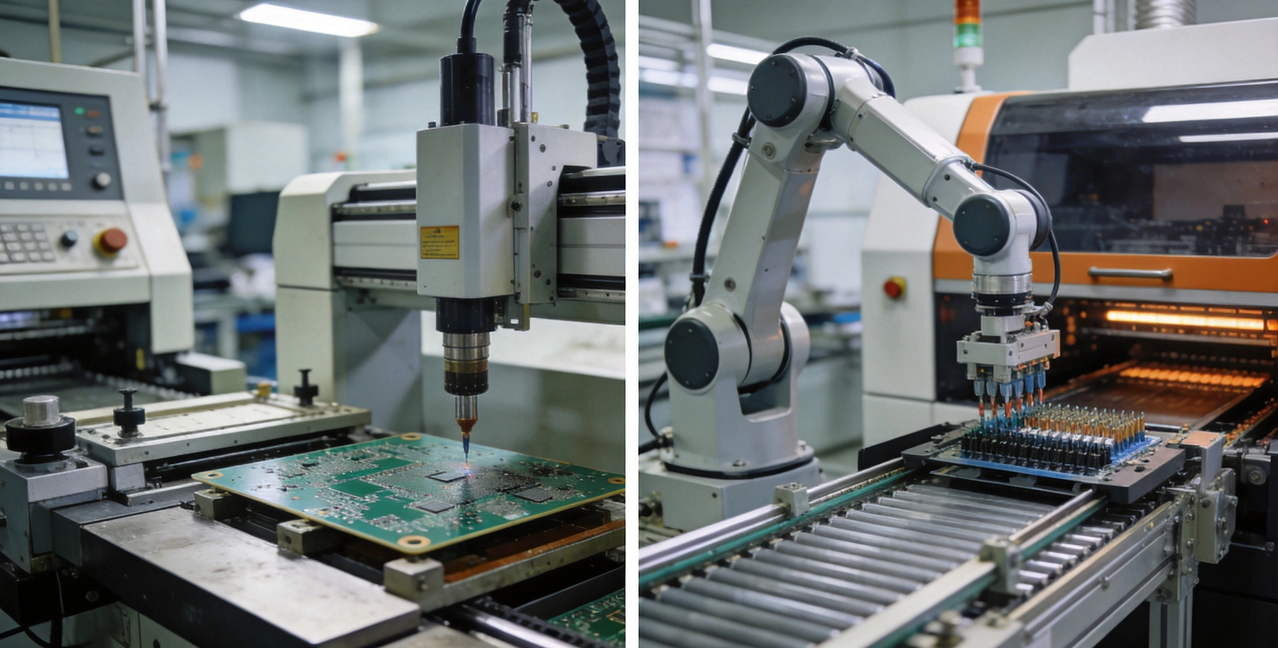
PCB Fabrication is the process of taking a set of design files and transforming raw laminate material into a finished bare board — a board with copper traces, drilled holes, plated vias, solder mask, and surface finish, but no components yet. The output of fabrication is what engineers call the "bare board" or "naked Pcb."
Fabrication starts with the laminate — a composite material typically made from woven glass fabric impregnated with an epoxy resin (FR4 is the most common grade). The process goes through a sequence of steps that transform this flat sheet into a complex multilayer interconnect structure.
The key steps in Pcb Fabrication are:
Inner Layer Processing: For multilayer boards, the inner copper layers are etched first. A photosensitive dry film is applied to the copper surface, exposed to UV light through a phototool generated from the design files, and developed to reveal the circuit pattern. The unwanted copper is then etched away, leaving the traces and pads that form the circuitry on that layer.
Lamination: The etched inner layers and prepreg (partially cured glass-reinforced epoxy sheets) are stacked in a precise alignment fixture and laminated under heat and pressure. This bonds all the layers together into a unified board substrate. For boards with blind or buried vias, this step is repeated multiple times with intermediate drilling and plating operations — a process called sequential lamination.
Drilling: Holes are drilled through the laminated board stack at the locations specified in the design files. These include through-hole vias that connect all layers, and for HDI boards, laser-drilled microblind vias that connect only specific layers. Drill accuracy is critical — the positional accuracy of holes directly affects whether the finished board will assemble correctly and function reliably.
Plating: After drilling, the board goes through an electroless and electroplating process that deposits copper on the walls of the drilled holes, creating the conductive barrel that connects layers. The quality of this plating — thickness, uniformity, void-free coverage — is one of the most important determinants of board reliability.
Outer Layer Imaging and Etching: The outer copper layers are imaged and etched using the same process as the inner layers, forming the top and bottom circuit patterns.
Solder Mask: A photosensitive solder mask coating is applied over the entire board surface, exposed, and developed to leave openings over the component pads where components will be soldered. The solder mask protects the copper traces from oxidation and prevents accidental solder bridges during assembly.
Surface Finish: The exposed copper pads receive a surface finish to protect them from oxidation and to provide a solderable surface for assembly. Common finishes include ENIG (electroless nickel immersion gold), HASL (hot air solder leveling), OSP (organic solderability preservative), and immersion silver. The choice of surface finish affects solderability, shelf life, and cost.
Electrical Testing: Before the bare board ships, it is tested for opens, shorts, and netlist verification to confirm that all the connections defined in the design files are actually present in the manufactured board.
Pcb Fabrication is performed by a fab house — a specialized manufacturer with equipment for drilling, plating, imaging, and lamination. Most fab houses do not perform component assembly. They produce bare boards and ship them to either the customer or to an assembly partner. Some manufacturers operate both fab and assembly capabilities in the same facility, which can simplify logistics but does not change the technical distinction between the two processes.
pcb assembly — often abbreviated PCBA (Printed Circuit Board Assembly) — is the process of placing components onto the bare board and soldering them to create a functional electronic circuit. Where fabrication ends with a bare board, assembly begins with one.
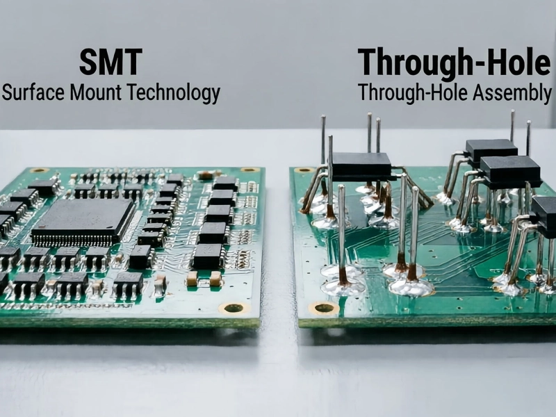
Modern Electronics Assembly is predominantly Surface Mount Technology (SMT), though through-hole technology (THT) is still used for connectors, transformers, and components that require mechanical robustness or high current handling. Many products use a combination of both.
Solder Paste Printing: Before components are placed, a stencil is used to apply Solder Paste to the component pads on the board. The stencil is a thin metal sheet with laser-cut openings that match the pad pattern. Solder Paste is a mixture of powdered solder suspended in flux, and the quality of the paste print — deposit volume, alignment, consistency — has a direct effect on the solder joint quality. Automated Optical Inspection (AOI) of the printed paste is increasingly standard in quality-focused assembly facilities.
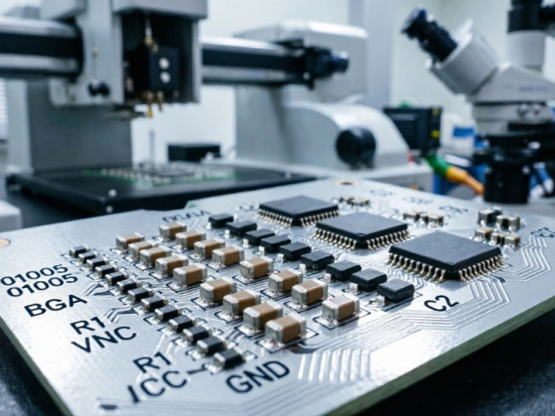
Component Placement: After paste printing, the board moves to the pick-and-place machine, which picks components from feeders or trays and places them precisely on the pads. Modern high-speed pick-and-place systems can place tens of thousands of components per hour with placement accuracy of ±0.05 mm or better. For fine-pitch BGAs, 0201 and 01005 passive components, and ultra-small Qfn packages, placement accuracy is critical — a misplacement of even a few tenths of a millimeter can cause a failed solder joint or a short.
Reflow Soldering: After placement, the board passes through a reflow oven — a conveyorized furnace with multiple temperature zones that heat the board in a controlled profile. The profile is designed to melt the solder paste, form a metallurgical bond with the component terminations and pad surfaces, and then cool at a controlled rate to solidify the joint. The reflow profile must be precisely matched to the board mass, component thermal mass, and the solder paste alloy being used. A profile that is too hot or too fast can cause component damage; one that is too cool or too slow can cause incomplete solder joints.
Through-Hole Insertion (if applicable): For boards that include through-hole components, the THT parts are inserted after the SMT reflow pass — either manually or using radial/axial insertion equipment — and then soldered using Wave Soldering or selective soldering, depending on the board design and the components present.
Inspection and Test: After soldering, the assembled board goes through inspection to verify solder joint quality and component placement accuracy. AOI systems inspect for Missing Components, misplacements, Tombstoning, bridging, and other assembly defects. For boards with hidden solder joints under Bga or Qfn packages, X-ray inspection is required to verify the integrity of the solder joint beneath the component body. The board then undergoes electrical testing — either in-circuit testing (ICT), flying probe testing, or functional testing (FCT) — to verify that the board performs its intended electrical function.
Pcb Assembly is performed by an EMS (Electronics Manufacturing services) provider, also called an assembly house or Contract Manufacturer. Like fab houses, some assembly providers are large-scale operations with multiple production lines and thousands of employees, while others are smaller job shops focused on prototypes, low-volume production, or highly specialized applications.
Understanding the difference between fabrication and assembly matters for two practical reasons: sourcing and communication.
If you source fabrication and assembly separately, you act as the intermediary — you receive bare boards from the fab, arrange shipping to the assembly house, manage the Component Procurement, and coordinate the schedule between two vendors. This gives you more visibility and control, but it also adds complexity, cost, and risk. A delay at the fab house cascades into a delay at the assembly house. A quality issue on the bare board may not be discovered until assembly reveals a plating void or an out-of-tolerance impedance.
Turnkey Assembly services consolidate both processes under one roof. The turnkey provider receives your design files and Bill Of Materials (BOM), procures components, fabricates the bare boards, assembles the components, tests the finished boards, and ships them to you. For most buyers — especially those without an internal Supply Chain team experienced in Pcb logistics — the turnkey model is more efficient and lower risk.
The tradeoff is reduced visibility into the detailed fab and assembly process. A good turnkey provider will give you the information you need (first article reports, inspection images, test data) without burdening you with the details you do not need. But if your project has unusual requirements that require tight control over specific fabrication parameters, a split-sourcing approach may give you the access you need.
When you understand the distinction between fab and assembly, you communicate more effectively with your Manufacturing partners. If you tell an assembly house that you need "the board fabbed to IPC Class 2," they may not be the right person to ask — that specification applies to the fab process, not the assembly process. Conversely, if you describe an assembly problem to a fab engineer, they may not have the context to diagnose it effectively.
Knowing which process is relevant to which question — plating thickness and material specs are fabrication questions; paste volume and reflow profile are assembly questions — helps you get faster and more accurate answers when problems arise.
One of the most common sources of confusion and conflict in electronics manufacturing is the bare board acceptance process. When a fab house ships bare boards to an assembly house or a customer, the receiving party inspects the boards before accepting them into assembly. If the boards have defects — out-of-tolerance features, damaged solder mask, plating issues — the assembly house may reject them, which triggers a respin at the fab and a delay in the production schedule.
The best way to avoid bare board acceptance disputes is to define clear Acceptance Criteria in advance, typically using the IPC-600 acceptability standard for bare boards. This standard defines the criteria for what constitutes an acceptable board, including criteria for conductor width, spacing, annular ring, plating quality, solder mask coverage, and surface finish. Agreeing on IPC-600 class (Class 1 for consumer electronics, Class 2 for general industrial, Class 3 for high-reliability applications) at the start of the project eliminates ambiguity and prevents disputes.
A first article is a small initial production run — often just one to five boards — that is used to verify that the manufacturing process is producing boards that meet the design intent and the agreed-upon Acceptance Criteria. First article inspection (FAI) applies to both the bare board and the assembled board. For the bare board, FAI includes dimensional measurement, cross-section analysis, and netlist testing. For the assembled board, FAI includes Visual Inspection, X-ray inspection of hidden joints, and electrical testing against the full test plan.
Skipping the first article step to save time is one of the most common causes of production-scale problems. A respin of 1,000 assembled boards because a design issue was not caught in first article is far more expensive than a one-week delay to complete first article inspection properly.
Prototyping and small batch (1–50 units): Turnkey is almost always the right choice. The logistics of splitting fab and assembly across two vendors for a prototype run rarely make sense. Look for a turnkey provider with a quick-turn capability that can deliver prototype boards in days, not weeks.
Medium volume production (100–1,000 units): Turnkey remains the practical default for most projects, particularly if the BOM contains a mix of standard and specialized components. The assembly provider's purchasing volume gives them better component pricing and faster lead times than most individual buyers can achieve.
High volume production (10,000+ units): At high volumes, the economics shift. Some buyers prefer to separate fab and assembly to have direct control over the fab house relationship and potentially negotiate better pricing for each process independently. Others stay with turnkey because the operational simplicity and single-source accountability are worth the premium. The right choice depends on your internal engineering and Supply Chain capabilities.
Fab-only (boards only, no assembly): Some buyers — particularly those with in-house assembly capabilities or those who ship boards as standalone products — need only the bare board. In this case, sourcing from a dedicated fab house with strong quality systems is the appropriate approach.
PCB fabrication and Pcb Assembly are distinct manufacturing processes that turn a design concept into a finished product through sequential steps. Fabrication builds the bare board from raw laminate. Assembly adds components and solders them to create a functional circuit. Understanding what each process involves — and where one ends and the other begins — helps you make better sourcing decisions, communicate more effectively with manufacturing partners, and avoid the common pitfalls that come from ambiguity about who is responsible for what.
Whether you choose a turnkey provider that handles both, or a split-sourcing approach with separate fab and assembly partners, the key is to define the handoff points, acceptance criteria, and quality standards upfront. A clear agreement on those basics is what makes every project after it — simple or complex — run smoothly.
Contact us to discuss your requirements.
Turnkey vs. Consignment PCB Assembly: Which Model Fits Your Project?August/08/2026
What is PCB Assembly? A Beginner's Guide to the BasicsMay/22/2026
A Simple Explanation of Wave Soldering for Mixed-Technology BoardsJuly/22/2026

What is Reflow Soldering and Why Does the Temperature Profile Matter?July/14/2026
The Role of Conformal Coating in Protecting Your ElectronicsAugust/14/2026
Common PCB Assembly Defects and How to Spot Them VisuallyJuly/30/2026
What is the difference between Surface Mount Technology (SMT) and through-hole assembly?June/04/2026
Handling 01005 Components and Micro BGAsJune/03/2026