Open Nav


Every electronics manufacturer claims to deliver quality. What separates the exceptional from the merely adequate is the systematic approach to verifying it. Quality Assurance in pcb assembly extends far beyond a cursory visual check under a workbench lamp. It requires layered inspection technologies that catch different defect types at different stages of production, from Bare Board arrival through final functional verification. When a manufacturer promises comprehensive Quality Assurance using AOI, X-ray, and functional testing, that promise reflects a specific commitment to detecting problems before they reach customers.
This article explains how each inspection technology works, what defects it catches, and why the combination of all three forms a robust quality assurance framework that protects both manufacturers and end customers from the consequences of defective electronics.
The complexity of modern Pcb assemblies has increased dramatically alongside the proliferation of compact, feature-rich electronic products. Dense component placements with Bga, Qfn, and01005 passive packages leave little room for Manufacturing errors. A solder joint that appears superficially acceptable under manual inspection may harbor hidden voids, insufficient solder, or bridging defects that cause field failures weeks or months after the product ships.
Field failures carry costs that far exceed the original assembly expense. Product returns damage brand reputation, customer support expenses accumulate rapidly, and in safety-critical applications such as automotive or medical electronics, defective assemblies create liability exposure that no company wants to face. Quality assurance investments during Manufacturing represent the most cost-effective point for defect detection, where correction costs remain low and remedies remain straightforward.
Industries with stringent reliability requirements have driven quality assurance innovation for decades. Aerospace and Automotive Electronics pioneered rigorous inspection standards that have progressively influenced consumer Electronics Manufacturing. Today, even modestly priced products benefit from inspection capabilities originally developed for mission-critical applications.
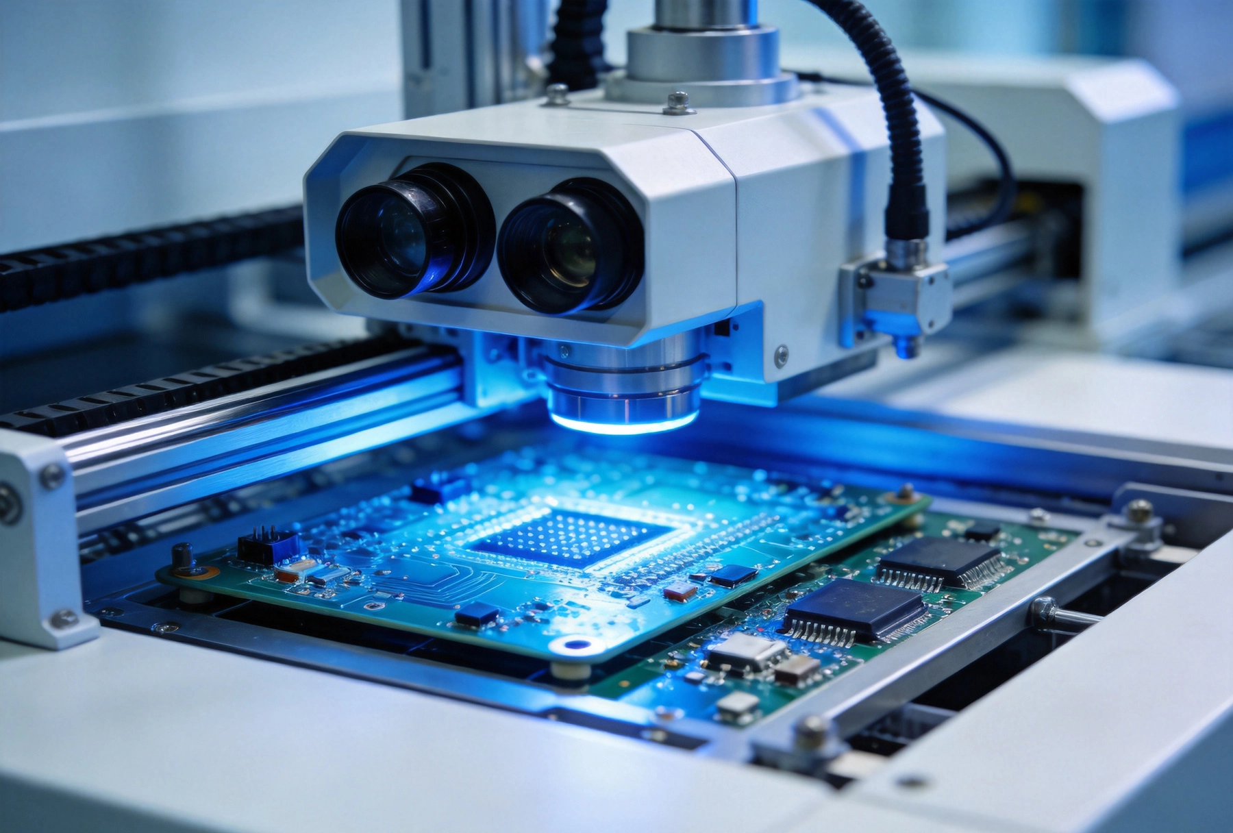
Automated Optical Inspection uses high-resolution cameras positioned above and sometimes below Pcb assemblies to capture images of component placement and solder joints. Sophisticated software algorithms compare captured images against stored reference images, identifying deviations that indicate defects such as Missing Components, misaligned placements, Tombstoning, solder bridges, insufficient solder, and component damage.
Modern AOI systems employ multiple lighting techniques to highlight different defect types. Coaxial lighting illuminates directly through the camera lens, revealing surface defects and component markings. Structured lighting at angles highlights solder joint geometry and detects coplanarity issues with leaded components. UV lighting reveals Conformal Coating coverage and identifies counterfeit components with altered date codes.
Resolution requirements scale with component density. Assemblies with 0201 or 01005 passives and fine-pitch QFP packages require AOI cameras capable of resolving features below 20 micrometers. Systems with 10-15 megapixel sensors and precision optics meet these requirements, though at corresponding cost and processing time investments.
Aoi Inspection typically occurs at multiple points in the assembly process. Post-paste inspection (API) examines the PCB after Solder Paste application, verifying stencil release and detecting insufficient or excessive paste that would cause assembly problems downstream. This early inspection catches the majority of paste-related defects before expensive components are placed.
Post-placement inspection follows component mounting but before Reflow Soldering, verifying that all components are correctly placed and oriented. This inspection catches placement errors, swapped components, and polarity reversals before thermal processing locks them into the board permanently. Since correction at this stage simply requires desoldering and repositioning, costs remain minimal.
Post-reflow inspection represents the most common AOI checkpoint, examining finished solder joints after the thermal profile has been completed. Defects identified at this stage require rework, including solder removal, component extraction, and re-processing. While more costly than pre-reflow corrections, rework remains far less expensive than field returns.
AOI effectively detects visible defects on exposed surfaces, but cannot see through components or beneath packages where solder joints hide from optical inspection. Bga packages, Qfn devices with bottom-terminated leads, and other area-array packages create blind spots where defects remain invisible to camera-based inspection. Plated through-hole joints on multilayer boards may appear acceptable optically while harboring voids or cracks internally.
Algorithm tuning presents an ongoing challenge for AOI systems. Overly sensitive settings generate excessive false calls that slow production and require operator review time. Insensitive settings allow real defects to pass undetected. Finding the appropriate balance requires continuous adjustment based on defect escape rates measured through downstream inspection stages.
X-ray inspection penetrates materials that block visible light, revealing internal structures hidden beneath component packages and PCB layers. Different materials absorb X-rays at different rates based on atomic density, creating contrast in radiographic images that distinguishes solder from component bodies, copper traces from substrate, and voids within solder joints from solid metal.
Two primary X-ray technologies serve PCB inspection needs. 2D X-ray systems capture flat projected images similar to medical radiographs, useful for identifying gross defects and reviewing hidden features. 2D imaging remains limited for complex assemblies where overlapping structures obscure individual features of interest.
Computed Tomography (CT) X-ray systems capture multiple images from different angles and reconstruct three-dimensional representations of internal structures. CT inspection enables precise measurement of void content, solder fillet geometry, and layered structure relationships. While CT provides superior analysis capability, scan times of several minutes per board limit throughput compared to 2D systems.
2.5D X-ray systems offer a practical middle ground, tilting assemblies during imaging to reveal internal features obscured in straight-on views. This technique works well for BGA inspection where oblique angles reveal ball connections without requiring full CT reconstruction.
Solder voiding represents the most common BGA and QFN defect identified through X-ray inspection. Voids form when volatiles become trapped during reflow, creating internal cavities that reduce mechanical strength and thermal conductivity. Ipc Standards specify maximum void percentages for different application categories, with Class 3 aerospace applications limiting voids to under 5% of joint area in critical locations.
Solder Bridging between adjacent joints causes electrical shorts that fail assemblies immediately or create intermittent failures that prove maddening to diagnose. X-ray imaging reveals bridges hidden beneath component bodies that AOI cannot detect, particularly for fine-pitch devices where lead spacing approaches the resolution limits of optical systems.
Insufficient solder joints may appear adequate from above while containing inadequate fillet formation underneath. X-ray inspection quantifies actual solder volume and fillet geometry, ensuring joints meet mechanical strength requirements even when visual appearance suggests acceptable quality. Insufficient solder frequently traces to paste printing problems, inconsistent stencil release, or oxidation on component terminations.
Header and connector alignment problems also reveal themselves through X-ray inspection. Press-fit connectors that do not fully insert, header pins that miss plated through-hole barrels, and misaligned connectors that create offset connections all become visible when X-ray imaging penetrates these assemblies.
X-ray equipment represents significant capital investment, with capable systems starting above $150,000 and advanced CT systems reaching $500,000 or more. This investment limits X-ray inspection to targeted applications where hidden defect detection justifies the cost, rather than screening every assembly produced.
Throughput constraints mean X-ray inspection typically serves as a sampling tool rather than 100% screening for high-volume production. Statistical process control approaches use X-ray inspection to monitor process stability, examining sample boards from each production lot to verify continued capability. Significant shifts in X-ray sample results trigger root cause investigation before defective boards contaminate production output.
Image interpretation requires trained technicians who understand both normal variation in manufacturing processes and defect signatures that indicate problems. Misinterpretation can lead to unnecessary rework of acceptable assemblies or acceptance of assemblies with borderline defects that may cause field failures.
Functional testing applies power and signals to assembled PCBs while monitoring performance against specification requirements. Unlike inspection technologies that examine physical characteristics, functional testing verifies that assemblies actually perform their intended functions correctly. A board with perfect solder joints and correctly placed components may still fail if component values are wrong, firmware is corrupted, or subtle interactions between components create performance problems.
Functional test approaches vary based on product complexity and test coverage requirements. Basic functional tests verify power supply operation, processor boot, and simple indicator responses. Comprehensive tests exercise all circuit functions, including analog signal paths, communication interfaces, RF performance, and edge case conditions that stress system boundaries.
In-circuit testing (ICT) uses a bed-of-nails fixture to access circuit nodes directly, measuring component values and verifying connections without requiring the full circuit to operate. ICT catches component placement errors, wrong component values, opens in circuit paths, and shorts between adjacent nodes. ICT provides thorough coverage but requires expensive fixtures and longer test development time.
Modern complex ICs with hundreds of pins present challenges for traditional physical probe-based testing. Boundary Scan technology, standardized as IEEE 1149.1, embeds test access circuitry within ICs themselves, enabling test vectors to shift data in and out through serial chains rather than requiring physical access to each pin.
Boundary Scan effectively tests interconnections between ICs without requiring functional operation of the chips themselves. This capability proves invaluable for assemblies where functional testing would require complex software loading or expensive test equipment. Missing connections, solder bridges, and open circuits on boundary scan pins all become detectable through JTAG interface access.
Assemblies without boundary scan capability on critical ICs face more limited test coverage through physical probing, fixture-based functional test, or burn-in stress testing that accelerates latent defect manifestation.
Burn-in testing operates assemblies at elevated temperature with power applied for extended periods, accelerating failure mechanisms that would otherwise manifest only after months of field operation. Components with latent defects, marginal solder joints, and weak internal connections fail during burn-in before shipping to customers.
Temperature cycling exposes assemblies to repeated heating and cooling that expands and contracts solder joints and component materials at different rates. Differential expansion creates mechanical stress that cracks weak joints, delaminates PCB layers, and separates component terminations from bodies. Cycling between temperature extremes faster reveals these problems than field operation in stable environments.
Highly accelerated stress testing (HAST) combines elevated temperature and humidity to accelerate moisture-related failure mechanisms. Assemblies that pass HAST testing demonstrate resilience to humid environments without the time investment of natural aging.
No single inspection technology catches all defect types. AOI misses hidden defects that X-ray reveals. X-ray inspection cannot verify actual circuit functionality. Functional testing may pass assemblies with marginal solder joints that Thermal Stress would eventually break. The power of comprehensive quality assurance emerges from combining these technologies strategically throughout the production process.
Production flow design places each inspection technology at the point where it provides maximum value. Early AOI catches manufacturing process problems immediately, enabling rapid feedback to adjust paste printing, placement programming, and reflow profile parameters. X-ray inspection of samples verifies process stability and catches random defects that statistical variation introduces. Functional testing provides final confirmation that assemblies meet performance specifications before shipping.
Inspection data flows back to process engineering teams who analyze defect patterns and trends to drive continuous improvement. When AOI data shows increasing component placement errors, placement machine maintenance or feeder issues require investigation. When X-ray samples reveal rising void percentages, paste printing or reflow profile adjustments address the root cause.
When a pcb assembly manufacturer promises comprehensive quality assurance using AOI, X-ray, and functional testing, that promise translates into tangible benefits for your products and business. Reduced field failure rates mean fewer customer returns, lower support costs, and preserved brand reputation. Consistent quality means predictable performance across production batches, enabling reliable product roadmaps and customer commitments.
Traceability documentation connects inspection results to specific boards, enabling targeted root cause analysis when field problems emerge. Lot-level traceability identifies which production runs may require customer notification or recall actions, reducing the scope of quality concerns while demonstrating responsible response to issues.
Quality assurance investments do increase manufacturing costs, but these costs represent insurance against far larger expenses from field failures, warranty claims, and reputation damage. The cheapest assembly quote often proves most expensive when viewed across total product lifecycle costs.
Automated Optical Inspection provides fast, thorough screening of visible defects across 100% of production, catching paste problems, component placement errors, and solder defects before they compound into more serious issues. X-ray inspection penetrates the hidden spaces where BGA, QFN, and area-array packages conceal defects from optical inspection, verifying internal solder joint integrity through the manufacturing process. Functional testing confirms that assemblies actually work as intended, exercising circuits under real operating conditions and catching problems that inspection alone would miss.
These three technologies form an integrated quality assurance system that protects both manufacturers and customers from the consequences of defective electronics. When evaluating assembly partners, understanding their inspection capabilities and how they deploy these technologies throughout production reveals the true depth of their quality commitment.
AOI can only inspect surfaces visible to cameras, leaving defects hidden beneath BGA packages, QFN bottom-terminated leads, and multilayer board internal structures. Relying solely on AOI allows hidden solder joint defects to pass undetected, potentially causing field failures in deployed products.
X-ray inspection frequency depends on product reliability requirements and process stability. High-reliability products may warrant 100% X-ray inspection, while consumer products often use statistical sampling approaches. Process monitoring typically examines 5-10 sample boards per lot, with increased sampling when process shifts are detected.
Functional testing identifies problems with component values, firmware corruption, incomplete programming, subtle circuit interactions, and performance that falls within specification tolerances but indicates impending failure. Some electrical defects only manifest under actual operating conditions that inspection technologies do not replicate.
Industry studies consistently show that field failure costs range from 10 to 100 times higher than equivalent defects caught during manufacturing, depending on product complexity, failure severity, and customer impact. Reworking a single assembly at the manufacturing stage typically costs under $20, while field returns often exceed $200 in logistics, repair, and customer relationship costs.
Small operations can implement effective quality assurance with appropriately scaled inspection equipment. Lower production volumes may justify Visual Inspection combined with selective AOI rental or service bureau inspection. The key factor is systematic application of multiple inspection technologies rather than reliance on any single method.

What to Expect from PCB Assembly Shenzhen SuppliersOctober/14/2026

Welcome to Our PCB Assembly Services Hub: Your Resource CenterMay/22/2026
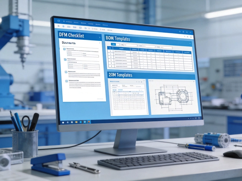
Downloadable Resources: DFM Checklists and BOM TemplatesAugust/03/2026
Customer Success Stories: Real Projects Delivered by Our TeamJuly/17/2026
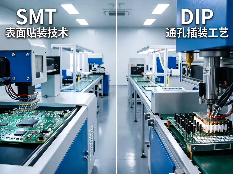
Comprehensive Guide to Our SMT and DIP CapabilitiesJune/09/2026
How We Handle Rush Orders and Quick-Turn PCB PrototypingJuly/08/2026
Requesting a Quote: A Step-by-Step Walkthrough for New ClientsSeptember/17/2026

Meet the Team: Expertise Behind Our High-Yield Production LinesSeptember/02/2026