

Wave Soldering represents one of the most efficient and cost-effective methods for soldering through-hole components on printed circuit boards. But what happens when your board combines both Surface Mount Technology (SMT) components and traditional through-hole parts? This common scenario, known as mixed-technology assembly, requires special consideration to ensure successful Wave Soldering without damaging sensitive SMT components. Understanding how wave soldering works with mixed-technology boards helps you design better products, choose appropriate Manufacturing processes, and avoid common pitfalls that can compromise quality and reliability.
This guide provides a straightforward explanation of wave soldering specifically for mixed-technology boards, breaking down the process into understandable concepts, exploring practical considerations, and offering actionable insights for engineers, designers, and anyone interested in Electronics Manufacturing.
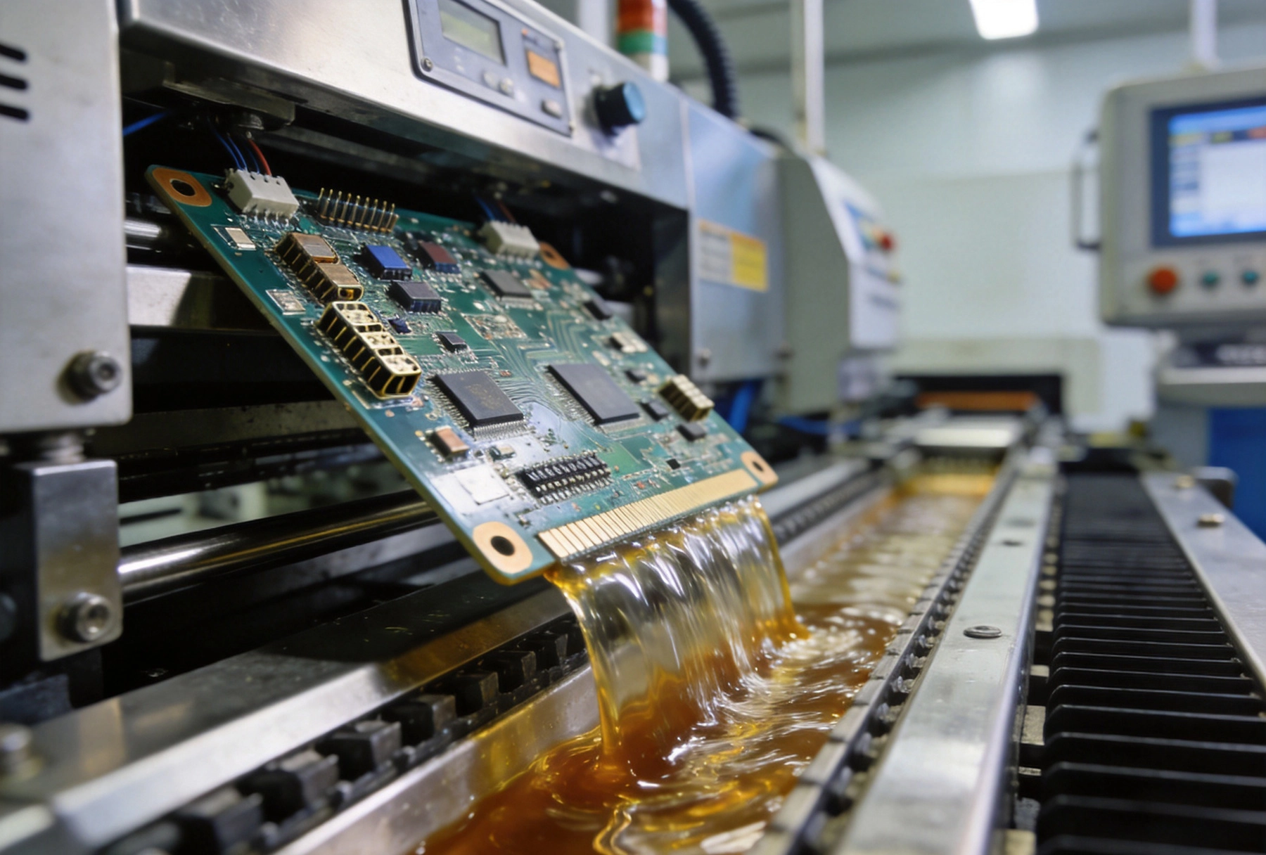
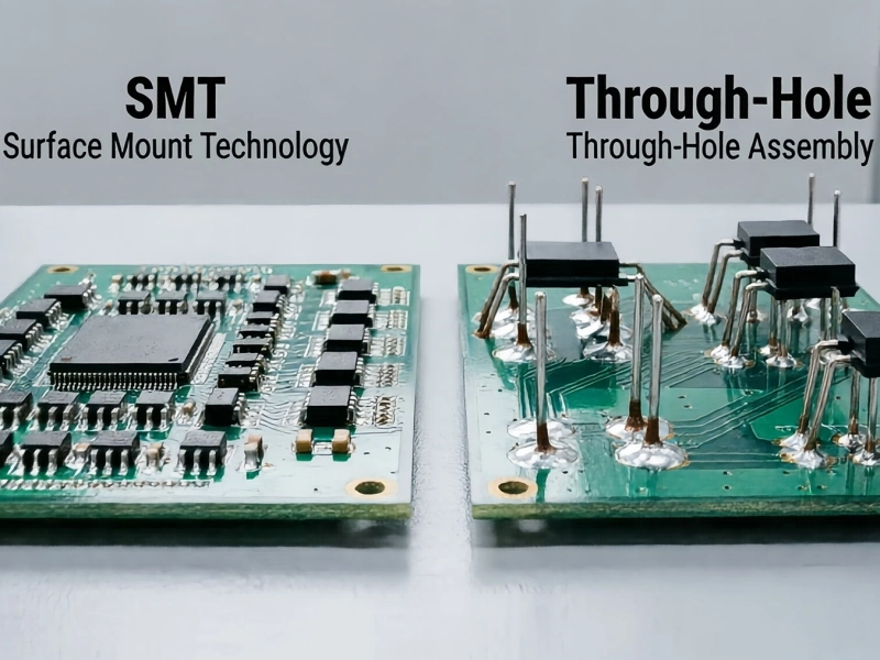
Before diving into wave soldering specifics, it's important to understand what mixed-technology boards are and why they're so common in modern electronics. Mixed-technology boards combine two types of Electronic Components on the same printed circuit board:
SMT components mount directly onto the surface of PCBs without requiring holes through the board. These components typically have small metal terminals or solder balls that make electrical contact with copper pads on the board surface. Common SMT components include resistors, capacitors, integrated circuits in various packages (SOIC, QFP, Bga), and many others. SMT components are generally smaller, lighter, and更适合 automated assembly than their through-hole counterparts.
Through-hole components have wire leads that insert through holes drilled in the Pcb and are soldered to copper pads on the opposite side. These components include connectors, switches, large capacitors, transformers, relays, and various other parts that benefit from the mechanical strength provided by through-hole mounting. Through-hole components often handle higher currents, provide better mechanical connection, and are easier for manual assembly or field repairs.
Mixed-technology boards offer the best of both worlds. SMT components enable high density, automated assembly, and cost-effective production for the majority of electronic parts. Through-hole components provide mechanical strength, high current capability, and ease of manual assembly where needed. Many products naturally require both types—consumer electronics might use SMT for most circuitry but through-hole connectors for external interfaces, power supplies might use SMT for control circuitry but through-hole for power components, and industrial equipment often combines both for optimal performance and manufacturability.
Wave soldering is a bulk soldering process used to solder through-hole components to printed circuit boards. The process gets its name from the "wave" of molten solder that the board passes over, creating solder joints on all through-hole leads simultaneously. Think of it like dipping bread into melted cheese—the bread (Pcb) passes over the cheese (molten solder), and the cheese sticks to the bread where there are openings (through-holes).
The fundamental wave soldering process involves several key steps:
This entire process happens in a continuous conveyor system, with boards moving through the wave soldering machine at controlled speeds. Modern wave soldering machines can process hundreds of boards per hour, making them highly efficient for high-volume production.
The heart of wave soldering is, of course, the solder wave itself. Molten solder (typically a tin-lead or lead-free alloy) is pumped from a reservoir to create a standing wave that maintains a consistent height and shape. The PCB bottom side contacts this wave as it passes over, allowing solder to flow around component leads and form reliable solder joints. The wave shape and contact angle are carefully engineered to ensure proper solder penetration without creating solder bridges or other defects.
Modern wave soldering machines often feature multiple wave types for optimal results:
Wave soldering mixed-technology boards introduces a fundamental challenge: the process that perfectly solder through-hole components can damage or dislodge SMT components mounted on the bottom side of the board. When SMT components are present on the bottom surface, they're exposed to the same flux, preheat, and molten solder that processes through-hole components. This exposure creates several potential problems:
The physical force of the solder wave can knock loosely attached SMT components off the board. This is particularly problematic for components that haven't been securely attached or that have minimal Solder Paste holding them in place. The turbulent motion of molten solder creates hydraulic forces that can overcome the adhesive properties of uncured Solder Paste or weak mechanical connections.
Solder from the wave can create unwanted connections (bridges) between adjacent SMT component leads or pads. This is especially concerning for fine-pitch SMT components where lead spacing is minimal. Solder Bridging creates short circuits that can render the board non-functional or cause unreliable operation.
Wave soldering exposes boards to relatively high temperatures—typically 250-270°C for Lead-free Solder, slightly lower for tin-lead alloys. While most SMT components can withstand these temperatures for brief periods, prolonged exposure or repeated thermal cycling can damage sensitive components, particularly plastic-encapsulated parts or those with internal materials not designed for wave soldering temperatures.
Flux applied for wave soldering can leave residues on SMT components that may cause corrosion, electrical leakage, or cosmetic issues. Some flux types are more aggressive than others and may be incompatible with certain SMT component materials or conformal coatings applied after assembly.
Fortunately, several proven approaches address these challenges and enable successful wave soldering of mixed-technology boards:
The most fundamental solution is careful component placement design. The most reliable approach places all SMT components on the top side of the board only, leaving the bottom side exclusively for through-hole component leads that will contact the solder wave. This eliminates SMT component exposure to the wave entirely and represents the safest design approach for wave soldering mixed-technology boards.
When bottom-side SMT components are unavoidable, several strategies help minimize problems:
For boards with many bottom-side SMT components or very fine-pitch parts, selective soldering often provides a better alternative than traditional wave soldering. Selective soldering uses a small, precisely controlled solder fountain or nozzle that solders only specific through-hole locations, avoiding SMT components entirely. This approach eliminates wave-related damage risks while still providing reliable through-hole solder joints. However, selective soldering is typically slower and more expensive than wave soldering for high-volume production.
When wave soldering mixed-technology boards with bottom-side SMT components, careful process optimization becomes critical:
Implementing design for manufacturability principles specifically for wave soldering prevents many common problems:
Let's walk through the actual wave soldering process for mixed-technology boards step by step:
Before wave soldering, mixed-technology boards typically undergo Smt Assembly on the top side first. This involves applying solder paste, placing SMT components, and Reflow Soldering them on the top surface. Some designs may also include bottom-side SMT components that are glued in place at this stage using SMT adhesive. The adhesive cures during the top-side reflow process, securing bottom-side components for the subsequent wave soldering operation.
The prepared board enters the wave soldering machine, where flux is applied to the bottom surface. Flux serves several critical functions: it removes oxidation from metal surfaces, promotes wetting of solder, and helps prevent re-oxidation during heating. For mixed-technology boards, flux selection is particularly important—it must provide excellent soldering performance for through-hole leads while being compatible with any bottom-side SMT components present.
The board passes through one or more preheating zones that gradually raise its temperature. Preheating serves multiple purposes: it activates the flux, evaporates volatile solvents, reduces thermal shock when the board contacts the molten solder wave, and helps bring the board closer to soldering temperature. For mixed-technology boards, preheat temperature must be carefully controlled—high enough to properly activate flux but not so high as to damage SMT components, particularly any on the bottom side.
The critical moment arrives when the board contacts the solder wave. The conveyor carries the board over the wave at a precisely controlled angle and speed. Molten solder flows up through the through-holes, around component leads, and creates the solder joints. If bottom-side SMT components are present, the solder wave contacts their terminations as well, potentially creating solder joints or causing problems depending on design and process parameters.
The wave contact time is typically just 2-5 seconds—brief enough to create proper solder joints without excessive heat exposure to components. The wave height, speed, and angle are all carefully tuned to achieve optimal results for the specific board design.
After passing over the solder wave, the board enters cooling zones where fans or other cooling methods rapidly reduce its temperature. Proper cooling is essential to solidify solder joints before the board experiences any mechanical stress. For mixed-technology boards, controlled cooling helps prevent thermal shock to SMT components and ensures reliable solder joint formation.
Completed boards undergo inspection to verify solder joint quality. Visual Inspection, Automated Optical Inspection (AOI), or X-ray inspection may be used depending on board complexity and quality requirements. Common defects to check for include solder bridges, insufficient solder, cold solder joints, tombstoned SMT components, or dislodged components. Any defects identified through rework or repair processes before the boards proceed to testing and final assembly.
Despite the challenges, wave soldering offers compelling advantages for mixed-technology boards:
Wave soldering processes boards continuously at high speed, making it one of the fastest methods for soldering through-hole components. A well-tuned wave soldering machine can process hundreds of boards per hour, far exceeding the throughput of manual soldering or selective soldering methods. This high throughput makes wave soldering ideal for high-volume production where cost efficiency is crucial.
When properly set up and maintained, wave soldering delivers highly consistent solder joint quality across all boards. The automated nature of the process eliminates variability introduced by manual soldering techniques. Process parameters like temperature, wave height, and conveyor speed can be precisely controlled and monitored, ensuring repeatable results board after board.
Wave soldering represents one of the most cost-effective methods for through-hole soldering, especially at higher volumes. The high throughput, low labor requirements, and efficient use of solder and flux all contribute to lower per-unit costs compared to alternative methods. While the initial equipment investment is significant, the ongoing operational costs are relatively low, making wave soldering economically attractive for volume production.
Wave soldering excels at soldering large through-hole components like connectors, terminal blocks, large capacitors, and power devices. These components often present challenges for other soldering methods but are handled easily by wave soldering's robust solder delivery system. The wave provides excellent hole fill and solder penetration even for large components with substantial thermal mass.
Wave soldering has been used in Electronics Manufacturing for decades, resulting in mature technology, well-understood processes, and widespread industry expertise. Equipment reliability, process knowledge, and troubleshooting capabilities are all well established, reducing implementation risks and supporting consistent quality outcomes.
Understanding common wave soldering defects helps prevent problems before they occur:
Problem: Unintended solder connections between adjacent leads or pads create short circuits.
Causes: Excessive solder, too much flux, incorrect wave height, or inadequate pad spacing.
Solutions: Reduce solder wave height, adjust flux application, optimize pad spacing in design, or implement design changes to increase clearance between conductors.
Problem: Through-hole leads don't receive enough solder to create reliable joints.
Causes: Inadequate wave contact time, low wave height, or improper preheating.
Solutions: Increase wave height, slow conveyor speed to extend contact time, or adjust preheat temperature to improve solder flow.
Problem: Solder joints appear dull, grainy, or cracked, indicating improper soldering.
Causes: Insufficient preheating, low solder temperature, or contamination.
Solutions: Increase preheat temperature, verify solder pot temperature, or improve board cleanliness before soldering.
Problem: Small SMT components stand up on one end instead of lying flat.
Causes: Uneven heating or solder wetting on component terminations.
Solutions: Optimize preheat uniformity, ensure balanced Pad Design, or use adhesive to secure components before wave soldering.
Problem: Bottom-side SMT components detach during wave soldering.
Causes: Insufficient adhesive, excessive wave force, or improper component orientation.
Solutions: Apply adequate SMT adhesive, reduce wave height, orient components parallel to wave direction, or relocate components to top side.
Follow these design guidelines to ensure your mixed-technology boards are suitable for wave soldering:
Implement comprehensive Quality Assurance to ensure reliable wave soldered assemblies:
Wave soldering makes sense for specific mixed-technology board scenarios:
Wave soldering remains a valuable process for mixed-technology boards, offering high throughput, consistent quality, and cost-effective production when properly applied. The key to success lies in thoughtful design that accounts for wave soldering requirements, careful process optimization, and comprehensive Quality Assurance. By understanding the challenges and implementing appropriate solutions, manufacturers can reliably produce high-quality mixed-technology assemblies using wave soldering technology.
As electronics continue evolving, wave soldering technology advances alongside it, with improved process control, better fluxes, and enhanced equipment capabilities. However, the fundamental principles remain the same: thoughtful design, proper preparation, controlled processing, and thorough inspection combine to produce reliable solder joints regardless of whether a board contains pure through-hole components or a mix of SMT and through-hole technologies.
For engineers and designers, the takeaway is clear: design with Manufacturing in mind from the start. Consider wave soldering requirements during PCB layout, select components compatible with the process, and communicate clearly with your manufacturing partners about your mixed-technology assembly needs. With this approach, wave soldering becomes an asset rather than a challenge in bringing mixed-technology products to market efficiently and reliably.
Yes, but with limitations. Small SMT components (typically 0805 size or larger) can be placed on the bottom side if secured with SMT adhesive. However, fine-pitch components, very small parts, or sensitive components should be avoided on the wave soldering side. The safest approach places all SMT components on the top side and reserves the bottom side exclusively for through-hole component leads.
Wave soldering temperatures depend on the solder alloy used. For traditional tin-lead solder (63/37), the solder pot typically operates at 255-265°C. For lead-free solders like SAC305 (96.5% tin, 3.0% silver, 0.5% copper), temperatures are higher, typically 260-270°C. Preheat temperatures usually range from 100-150°C, depending on board complexity and thermal mass.
Wave soldering conveyor speeds typically range from 3-6 feet per minute (1-2 meters per minute), though faster or slower speeds may be used depending on board requirements. At these speeds, a wave soldering machine can process 100-300 boards per hour or more, making it highly efficient for volume production. The exact speed depends on board size, thermal mass, and solder quality requirements.
Wave soldering processes entire boards simultaneously using a broad solder wave, making it fast and efficient for boards with many through-hole components. Selective soldering uses a small, precisely controlled solder nozzle that solders only specific locations, avoiding SMT components entirely. Selective soldering is slower and more expensive but necessary when boards have many bottom-side SMT components or require very precise soldering of specific through-hole locations.
Prevent solder bridging through design and process optimization. Ensure adequate pad spacing (minimum 0.050" between adjacent leads), apply appropriate flux amount, optimize wave height, and maintain proper conveyor speed. For fine-pitch through-hole components, consider using solder mask between pads or increasing spacing beyond minimum requirements. Process monitoring and regular inspection help identify bridging issues early for corrective action.
What is PCB Assembly? A Beginner's Guide to the BasicsMay/22/2026
Turnkey vs. Consignment PCB Assembly: Which Model Fits Your Project?August/08/2026
Common PCB Assembly Defects and How to Spot Them VisuallyJuly/30/2026
The Role of Conformal Coating in Protecting Your ElectronicsAugust/14/2026
What is the difference between Surface Mount Technology (SMT) and through-hole assembly?June/04/2026
PCB Fabrication and Assembly: What's the Difference?September/30/2026
What is Reflow Soldering and Why Does the Temperature Profile Matter?July/14/2026

How Automotive Electronics are Redefining PCBA Quality StandardsJuly/01/2026