Open Nav


Electronics Manufacturing has not historically been associated with environmental responsibility. The industry runs on hazardous chemicals, energy-intensive processes, and materials that are difficult to recycle. But that reality is shifting fast. Regulatory pressure, customer expectations, and genuine corporate responsibility are pushing pcb assembly toward greener processes — and the transition is more than a marketing exercise.
This article examines the Sustainability trends reshaping PCBA. We will look at Lead-free Solder adoption, halogen-free substrate alternatives, energy efficiency improvements on the factory floor, and what these changes mean for product reliability, cost, and supply chain decisions.
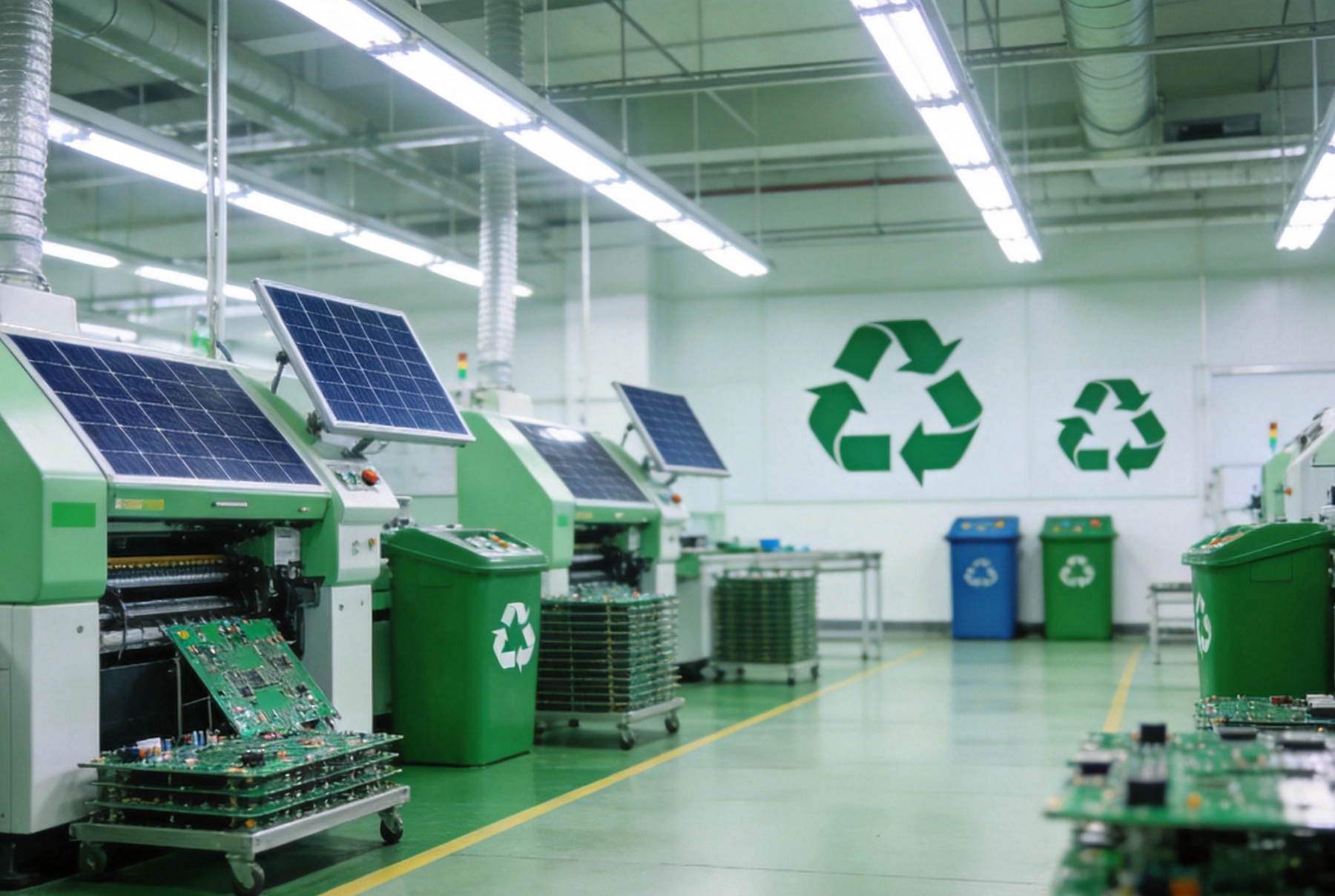
The electronics industry generates significant environmental impact across the product lifecycle. Raw material extraction for copper, gold, and rare earth elements carries environmental cost. Manufacturing consumes substantial energy and water, uses aggressive chemicals for etching and plating, and generates waste streams that require careful handling. End-of-life disposal poses challenges when devices end up in landfills and heavy metals leach into soil and groundwater.
Regulatory frameworks have responded. The European Union RoHS directive, in effect since 2006, restricts the use of lead, mercury, cadmium, hexavalent chromium, and certain flame retardants in electrical and electronic equipment. China, Japan, South Korea, and other major markets have implemented similar restrictions. These regulations have fundamentally changed what materials can be used in volume production.
Beyond compliance, customers are asking harder questions. Consumer electronics brands publish Sustainability reports and set carbon reduction targets. Industrial and automotive customers evaluate supply chain environmental performance as part of vendor qualification. For pcb assembly providers, sustainability is no longer a nice-to-have — it is a competitive requirement.
The most visible sustainability change in PCBA has been the shift from tin-lead solder to lead-free alternatives. Lead-free Solder is now the default for virtually all commercial electronics, driven by RoHS and similar regulations worldwide.
The most widely used lead-free alloy is SAC305 — tin, silver, and copper at 96.5 percent, 3.0 percent, and 0.5 percent respectively. This alloy offers reasonably good wetting, mechanical strength, and thermal fatigue resistance. It has become the standard choice for Smt Assembly and Reflow Soldering.
For Wave Soldering of mixed-technology boards, SAC alloys can be problematic due to copper dissolution from through-hole pads. Alternative alloys like SN100C (tin-copper-nickel with a small amount of germanium) offer better copper erosion resistance for Wave Soldering applications. The choice of alloy depends on the specific assembly process and the component mix on the board.
Lead-free solder has higher melting point than tin-lead. SAC305 melts at approximately 217 degrees Celsius, compared to 183 degrees Celsius for 63/37 tin-lead. This higher melting point requires higher reflow oven temperatures, which affects component stress, substrate materials, and energy consumption.
Lead-free solder also wets differently. The wetting angle is typically larger, meaning the solder fillet shape differs from tin-lead joints. This affects Visual Inspection criteria — a joint that looks suspicious under tin-lead standards may be perfectly acceptable under lead-free criteria. Ipc-a-610 includes separate Acceptance Criteria for lead-free solder joints.
Early concerns about lead-free solder reliability centered on tin whiskers — crystalline structures that grow from tin surfaces and can cause short circuits. Whisker risk is real, but it has been largely managed through alloy selection, plating choices, and Conformal Coating. Pure tin plating on component terminations is now common and reliable when properly specified.
Thermal cycling performance of lead-free joints is generally comparable to or better than tin-lead for most applications. However, lead-free joints can be more brittle under mechanical shock. For high-vibration or high-shock environments, careful joint design and appropriate solder alloy selection matter more than they did with tin-lead.
Traditional FR-4 substrates contain halogenated flame retardants — typically bromine compounds — to achieve the required flammability rating. When burned, these compounds can release toxic and corrosive gases. Halogen-free substrates use alternative flame retardant chemistries to eliminate this concern.
Halogen-free is defined by IEC 61249-2-21 as containing less than 900 parts per million of chlorine or bromine individually, and less than 1500 parts per million total halogens. Materials meeting this threshold can be labeled halogen-free.
Halogen-free substrates are not universally better for all applications. They typically have different mechanical and electrical properties from standard FR-4. The dielectric constant may differ. The thermal decomposition behavior may be less favorable for certain high-temperature applications. The cost is generally higher. Selecting halogen-free materials requires engineering evaluation, not just checkbox compliance.
Consumer electronics brands have been early adopters of halogen-free substrates, driven by sustainability commitments and product differentiation. Automotive applications are increasingly specifying halogen-free materials as well. The trend is real, but it is not yet universal across all product categories.
Sustainability extends beyond material choices. The assembly process itself consumes energy and resources. Progressive PCBA providers are addressing these impacts through operational improvements.
Reflow Soldering is one of the most energy-intensive steps in Smt Assembly. Modern reflow ovens use improved insulation, more efficient heating elements, and better zone control to reduce energy consumption. Nitrogen atmosphere reduces oxidation and can allow lower peak temperatures, which saves energy and reduces Thermal Stress on components.
Optimizing reflow profiles for the minimum acceptable peak temperature and time above liquidus also contributes to energy efficiency. This is a process engineering task that requires understanding the thermal mass of the product, the thermal mass of the oven conveyor, and the acceptable process window for the solder and components.
Wave soldering consumes substantial energy to maintain solder pot temperature. Selective soldering, which solders only the specific joints requiring through-hole termination, can reduce energy consumption for mixed-technology boards. The choice between wave and selective soldering involves throughput requirements, board complexity, and energy considerations.
PCB Fabrication uses significant water for rinsing between process steps. Assembly uses less water but still generates wastewater from cleaning operations. Water recycling, closed-loop systems, and wastewater treatment reduce the environmental impact of these processes. Responsible waste handling for solder dross, chemical containers, and other process byproducts is also part of sustainable operations.
Sustainability extends to how finished boards are packaged and shipped. Packaging materials — moisture barrier bags, desiccant, cardboard cartons, foam inserts — generate waste. Sustainable packaging uses recyclable or recycled materials, minimizes volume, and reduces the environmental footprint of logistics.
Transportation distance also matters. Regional Manufacturing reduces shipping miles and associated carbon emissions. Some companies are evaluating the Carbon Footprint of their supply chain and making sourcing decisions based partly on logistics distance. This is one factor behind the interest in regional PCB Fabrication and assembly capacity in North America and Europe, rather than relying exclusively on offshore production.
Sustainability initiatives often carry cost implications. Lead-free solder is more expensive than tin-lead due to the silver content. Halogen-free substrates cost more than standard FR-4. Energy-efficient equipment may have higher capital cost. These cost premiums are real, and they affect the economics of Pcb Assembly.
However, the cost gap is narrowing. Lead-free solder has been the default for nearly two decades in volume production; the process is mature and the cost differential is now marginal compared to the early transition years. Halogen-free substrates remain more expensive, but the price gap has narrowed as volumes have increased.
In many cases, sustainable processes offer offsetting benefits. Energy-efficient equipment reduces operating cost over time. Reduced hazardous material handling lowers compliance and disposal costs. Customers willing to pay for sustainability often have more stable supplier relationships and longer product lifecycles, which benefits the assembly provider as well.
The push toward sustainability is not without complications. Lead-free solder requires higher process temperatures, which can stress components and substrates. The reliability differences between lead-free and tin-lead solder are manageable but real, and they require engineering attention. Halogen-free substrates have different electrical and thermal properties that affect design decisions.
Supply chain complexity also increases. More material choices mean more specifications to manage, more qualification testing, and more potential for mix-ups. Documentation requirements increase. The sustainability benefits are real, but they do not come free.
For Pcb Assembly providers, the key is understanding which sustainability requirements apply to each customer and product. Not every board needs halogen-free substrate. Not every application requires the most aggressive sustainability certification. Matching the process to the actual requirement avoids unnecessary cost while meeting the specifications that matter.
Several standards and certification frameworks address sustainability in Electronics Manufacturing:
For customers evaluating assembly providers, asking about certifications provides insight into the maturity of their sustainability program. However, certification alone does not guarantee performance. The more meaningful indicator is how a provider discusses the trade-offs, process decisions, and engineering considerations that go into sustainable assembly.
Sustainability pressure will continue to increase. Regulatory requirements are expanding to cover more substances and more product categories. Customer expectations for Supply Chain Transparency are rising. Carbon reduction targets from major brands cascade down to component and assembly suppliers.
Emerging trends include increased use of recycled materials in substrate manufacturing, development of lower-temperature lead-free solder alloys to reduce energy consumption, and expanded use of Renewable Energy in manufacturing facilities. Digital tools for tracking and reporting environmental performance are becoming standard.
For engineers and sourcing professionals, the practical implication is that sustainability is now a standard consideration in Pcb assembly decisions. Understanding the material options, process implications, and cost trade-offs enables informed decisions that balance environmental responsibility with product performance and commercial reality.
For most commercial applications, yes. Lead-free solder joints have comparable thermal cycling reliability to tin-lead. Lead-free joints can be more brittle under mechanical shock, which matters for high-vibration applications. With proper joint design and appropriate alloy selection, lead-free solder provides reliable performance for the vast majority of electronic products.
Halogen-free substrates have different dielectric properties than standard FR-4, which affects impedance and signal integrity for high-frequency designs. They may have different thermal decomposition behavior. Cost is typically higher. For many applications, these differences are manageable, but they require engineering evaluation rather than simple substitution.
Yes. Lead-free solder joints have different wetting angles and fillet shapes than tin-lead joints. Ipc-a-610 includes separate acceptance criteria for lead-free joints. Inspectors need training to recognize acceptable lead-free joint characteristics and distinguish them from defects.
The cost impact varies by requirement. Lead-free solder adds minimal cost premium in volume production. Halogen-free substrates may add 10 to 30 percent material cost depending on the specific grade. Energy-efficient processes may have higher capital cost but lower operating cost over time. The total sustainability cost impact depends on which requirements apply to your specific product.
Lead-free assembly is now standard capability across virtually all commercial Pcb assembly providers. Halogen-free substrates, detailed sustainability reporting, and Carbon Footprint tracking are more commonly available from larger or more specialized providers. If specific sustainability requirements are important for your product, confirm capability during vendor qualification.
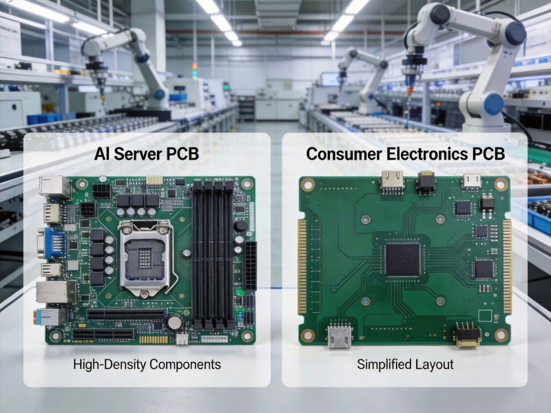
Navigating the Shift: Low-End vs. High-End PCB Assembly MarketsJune/12/2026
Why High-Reliability PCB Assembly is Critical for Medical DevicesJune/02/2026

The Rise of AI Servers and Their Impact on HDI PCB AssemblyJuly/10/2026

The State of Global PCBA Manufacturing in 2026 and Key TakeawaysMay/22/2026
Why High-Reliability PCB Assembly is Critical for Medical DevicesMay/22/2026
How Automotive Electronics are Redefining PCBA Quality StandardsJuly/01/2026
From Prototype to Mass Production: Scaling Your Hardware StartupSeptember/04/2026
Understanding the True Cost Drivers in Modern Electronics ManufacturingJuly/20/2026