
The pcb assembly landscape in 2026 looks markedly different than it did even three years ago. Supply chain disruptions have reshaped sourcing strategies, AI-driven inspection systems have transformed Quality Control, and the proliferation of advanced packages—fine-pitch BGAs, QFNs with bottom-side thermal pads, and chip-scale packages—has raised the technical bar for every assembly house. Meanwhile, economic pressures demand faster turns, lower costs, and zero-defect quality from prototype through production.
Whether you are a startup preparing for your first prototype build, an established OEM scaling to volume production, or an engineering manager evaluating assembly partners, understanding the current state of pcb assembly services is essential for making informed decisions. This guide covers the assembly process, service models, inspection technologies, quality frameworks, cost structures, and selection criteria that define Pcb Assembly services in 2026.

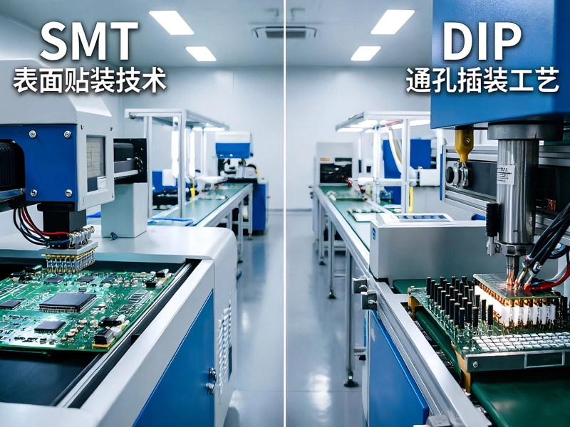
Every Pcb Assembly involves attaching components to a bare board and creating reliable solder joints. The two fundamental technologies—Surface Mount Technology (SMT) and through-hole technology (THT)—each have distinct advantages and assembly requirements.
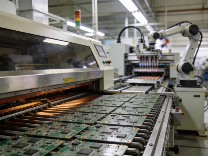
SMT is the dominant assembly technology, accounting for over 90% of components on a typical modern board. SMT components are soldered directly to pads on the board surface, enabling smaller footprints, higher component density, and automated assembly at high speed. The SMT process flow is:
In 2026, advances in SMT equipment include gantry-style placers with dual heads that achieve both high speed and high accuracy, reflow ovens with real-time Thermal Profiling capability, and solder paste printers with automatic stencil alignment and 3D paste inspection.
Through-hole components have leads that pass through drilled holes in the board and are soldered on the opposite side. THT provides superior mechanical strength—making it the choice for connectors, large capacitors, transformers, and any component subjected to mechanical stress. However, THT assembly is slower and more difficult to automate than SMT.
For through-hole soldering in 2026, the primary methods are:
Most real-world boards combine SMT and THT components. The typical mixed-technology process flow is:
This sequence requires careful process engineering to ensure that reflow cycles do not degrade previously soldered joints and that the wave/selective soldering step does not damage SMT components on the bottom side.
How components are sourced and inventory is managed defines the service model—a decision that significantly affects cost, lead time, risk, and Quality Control.
In Turnkey Assembly, the assembly house manages everything: procuring the bare boards, sourcing all components, assembling the boards, and performing inspection and test. You provide the design data (Gerber Files, BOM, and assembly drawings) and receive finished, tested boards.
Advantages:
Considerations:
In Consignment Assembly, you provide the bare boards and all components—kitted and ready for assembly. The assembly house provides only the labor, equipment, and process expertise.
Advantages:
Considerations:
Many projects use a hybrid approach: the assembly house sources commodity components while you consign specialized or proprietary parts. This combines the convenience of turnkey for readily available parts with the control of consignment for critical or scarce components. Clear documentation—which line items are turnkey and which are consigned—is essential to avoid confusion.
Quality control has undergone a transformation in recent years, driven by AI-powered inspection algorithms, 3D measurement capabilities, and the demand for zero-defect production in critical applications.
3D SPI systems measure the volume, height, and area of every solder paste deposit before components are placed. This catches printing defects—insufficient paste, excess paste, smearing, and offset deposits—at the earliest possible stage, when rework is cheapest. In 2026, AI-enhanced SPI systems learn from historical data to predict defect risk based on paste deposit geometry, enabling proactive stencil and process adjustments before defects actually occur.
AOI systems use high-resolution cameras and sophisticated image analysis algorithms to inspect boards after component placement and after reflow. AOI detects:
Modern AOI systems use multi-angle lighting and 3D height measurement to distinguish real defects from false alarms caused by component color variations, solder mask reflections, or board warpage. AI-based classifiers have dramatically reduced false call rates—the percentage of flagged "defects" that are actually acceptable—reducing the operator review burden and improving inspection throughput.
X-ray inspection is essential for verifying solder joints that are hidden from optical view—primarily Bga and Qfn packages where the joints are beneath the component body. AXI systems can detect:
In 2026, 3D computed tomography (CT) X-ray systems provide volumetric images that reveal defects impossible to detect with 2D projection—such as voids inside individual BGA balls that are overlapped by other balls in the 2D view. While CT inspection is slower and more expensive than 2D, it is increasingly used for high-reliability applications where the cost of a field failure justifies the additional inspection expense.
Post-soldering electrical verification catches defects that visual and X-ray inspection cannot—incorrect component values, open circuits, and functional failures. ICT uses a bed-of-nails fixture to access individual nets and measure component values, while FCT powers up the board and verifies that it performs its intended function. Flying probe testing provides ICT-like electrical verification without a dedicated fixture, making it cost-effective for prototypes and low-volume production.
The quality framework governing Pcb assembly is defined by a hierarchy of standards that specify acceptability criteria, process requirements, and Quality Management systems.
Ipc-a-610 "Acceptability of Electronic Assemblies" is the universal standard for judging whether a solder joint is acceptable. It defines three classes of acceptability:
Most assembly houses build to Class 2 by default. For Class 3, you must specify this requirement explicitly—it affects process parameters, inspection criteria, and cost.
Iso 9001 Certification demonstrates that the assembly house operates a Quality Management system. Beyond this baseline, industry-specific certifications may be required:
Understanding what drives assembly cost enables you to make design decisions that optimize the cost-performance tradeoff.
Setup costs are amortized over the production quantity. A stencil that costs $200 adds $0.20 per board at 1,000 units but $0.002 at 100,000 units. This is why prototype assembly is disproportionately expensive per unit—the fixed setup costs dominate. Volume price breaks typically occur at 100, 1,000, 5,000, and 10,000+ units as setup amortization, component volume pricing, and production efficiency all improve.
Assembly lead time—the calendar days from order placement to shipment—depends on several factors:
Typical lead times in 2026:
Artificial intelligence is transforming inspection from a rules-based process to a learning-based one. AI-trained AOI systems achieve lower false call rates and higher defect detection rates than traditional rule-based systems, particularly on complex boards with fine-pitch components where the variability of acceptable solder joint geometry makes rigid rules inadequate. Some assembly houses now offer AI-powered inspection as a standard service, with the AI models continuously improving as they process more boards.
The supply chain disruptions of recent years have driven a fundamental shift from just-in-time (JIT) single-source procurement to dual-source and regional-buffer strategies. Many assembly houses now maintain component inventory buffers—stocking critical components in anticipation of demand—rather than relying entirely on distribution network availability. This adds carrying cost but significantly reduces the risk of line-down situations caused by component shortages.
The drive toward smaller, more functional devices continues to push assembly capabilities. Component sizes of 0201 and 01005, once limited to mobile phone production, are now common in IoT, wearable, and medical device applications. Fine-pitch BGAs with 0.4mm ball pitch require placement accuracy and solder paste volume control that were considered specialized capabilities just a few years ago. Assembly houses that have invested in the equipment and process expertise for these advanced packages have a competitive advantage in 2026.
Environmental regulations continue to tighten. RoHS and Reach Compliance is now baseline—assembly houses must verify that all materials and processes meet these requirements and provide compliance documentation. Beyond compliance, many OEMs are setting Sustainability targets that include reduced energy consumption in Manufacturing, waste reduction, and the use of halogen-free materials. Assembly houses that can demonstrate environmental credentials—through Iso 14001 certification, Carbon Footprint reporting, or documented waste reduction programs—are increasingly preferred by Sustainability-conscious customers.
The digital transformation of assembly operations—Industry 4.0—accelerates in 2026. Smart factories use real-time data from SPI, AOI, and placement equipment to monitor process performance, predict maintenance needs, and optimize production scheduling. Digital twins—virtual models of the assembly process—enable process optimization without consuming production time or material. Traceability systems link every board to its component lots, process parameters, and inspection results, providing the comprehensive genealogy that quality standards and customers increasingly demand.
Selecting an assembly partner is a decision with long-term consequences. The right partner becomes an extension of your engineering team; the wrong one becomes a source of quality problems, missed deadlines, and frustration.
Can they actually build your board? Verify specific capabilities rather than accepting generic claims:
Beyond certifications, assess the quality culture:
Assembly is a collaborative process. Your partner should:
Your assembly partner must be financially stable enough to invest in equipment maintenance and upgrades, retain experienced staff, and weather economic fluctuations. They must also have sufficient capacity to handle your production volume without your orders becoming an afterthought. Visit the facility if possible—a factory tour reveals more about capability, organization, and culture than any capability statement.
Pcb Assembly Services in 2026 exist in a dynamic environment shaped by AI-driven inspection, supply chain restructuring, advancing component technology, and the relentless demand for higher quality at lower cost. The fundamentals—understanding SMT and THT processes, selecting the right service model, specifying appropriate inspection and quality requirements, and choosing a capable partner—remain as important as ever. But the tools, technologies, and best practices available to both assemblers and their customers have advanced significantly.
The most successful OEM-assembler relationships in 2026 are partnerships, not transactional vendor arrangements. Early engagement on DFM, transparent communication about requirements and constraints, and collaborative problem-solving when issues arise—these practices distinguish projects that flow smoothly from design through production from those that stumble at every handoff.
Whether you are building your first prototype or managing high-volume production, the principles in this guide will help you navigate the PCB assembly landscape and make decisions that deliver reliable boards, on time, at competitive cost.
Looking for a Pcb Assembly Partner equipped for 2026's challenges? Contact us to discuss your project requirements, tour our facility, and learn how our AI-enhanced inspection, turnkey capabilities, and ISO-certified quality system can support your next build.
Comprehensive Guide to Our SMT and DIP CapabilitiesJune/09/2026
Welcome to Our PCB Assembly Services Hub: Your Resource CenterMay/22/2026
Meet the Team: Expertise Behind Our High-Yield Production LinesSeptember/02/2026
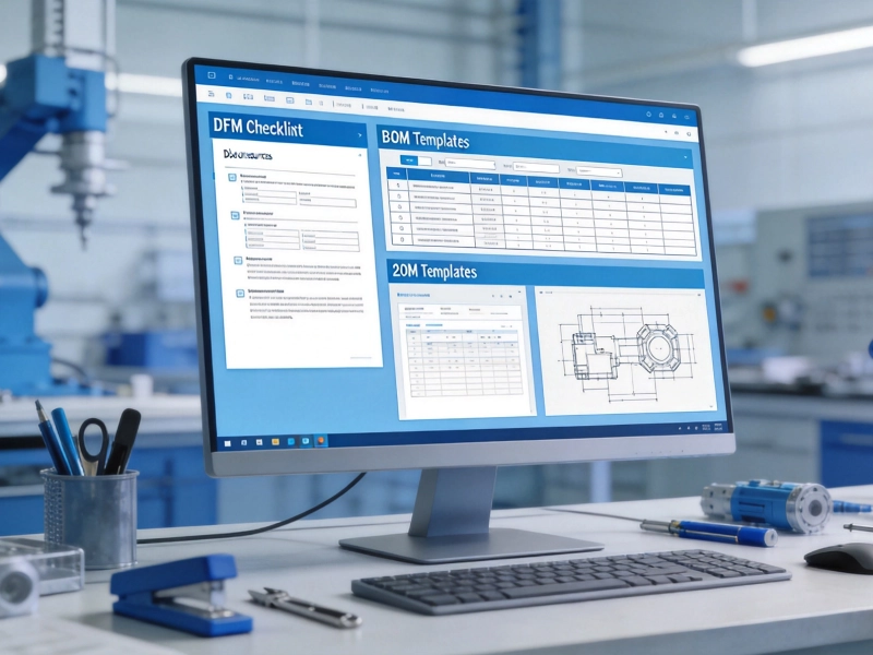
Downloadable Resources: DFM Checklists and BOM TemplatesAugust/03/2026
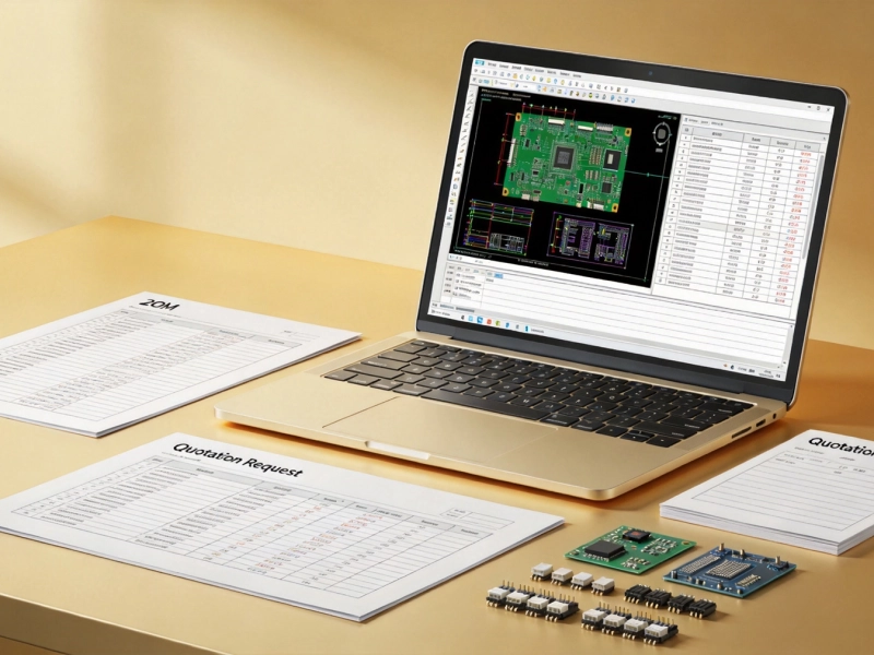
Requesting a Quote: A Step-by-Step Walkthrough for New ClientsSeptember/17/2026
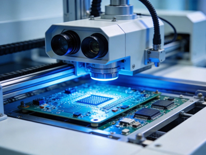
Our Quality Assurance Promise: AOI, X-Ray, and Functional TestingJune/26/2026
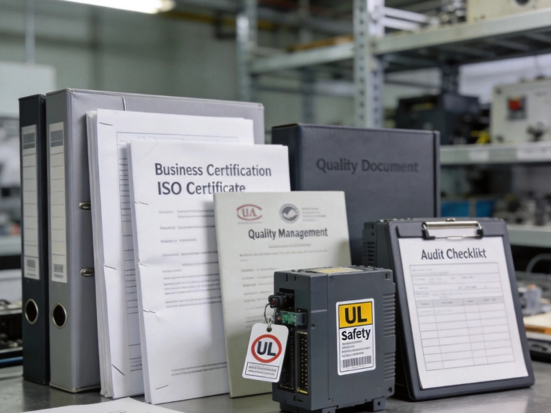
Certifications That Matter: ISO, IATF, and UL Compliance ExplainedSeptember/11/2026
Frequently Asked Questions About Our PCB Assembly ProcessJuly/25/2026