Open Nav


As electronic devices continue their relentless march toward smaller form factors and higher functionality, traditional surface-mount technology faces fundamental physical limitations. The transition from 0402 to 0201 to 01005 packages has pushed pick-and-place machines and Solder Paste Deposition to their precision limits. Yet market demands for thinner smartphones, smaller medical implants, and more compact IoT sensors show no signs of slowing. Embedded Component Technology (ECT) represents the next evolutionary step in Pcb miniaturization, moving components from the board surface into the internal layers of the substrate itself.
ECT fundamentally reimagines the relationship between components and the Pcb substrate. Rather than mounting discrete parts on the surface, passive and active components become integral elements of the board structure. This paradigm shift enables dramatic reductions in board area and thickness while simultaneously improving electrical performance by eliminating parasitic effects associated with surface-mount packages and solder joints. Understanding how this technology works, where it applies, and how to design for it positions engineers to create the ultra-compact products that next-generation applications demand.
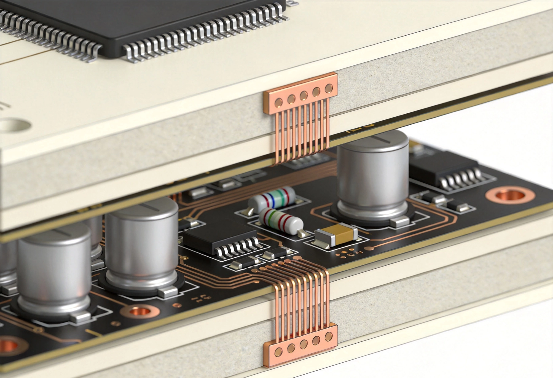
Embedded Component Technology encompasses several distinct approaches for integrating Electronic Components within the PCB substrate rather than mounting them on the surface. The technology spans both passive components, including resistors and capacitors, and active components such as integrated circuits and bare die. Each category presents different technical challenges and Manufacturing approaches, but all share the common goal of maximizing functional density within minimal physical volume.
The simplest form of ECT involves embedding passive components during the normal lamination process of multilayer PCB Fabrication. Thin-film resistors and capacitors are formed directly on internal copper layers using specialized materials and processes. These embedded passives occupy no surface area and add negligible thickness to the board, yet provide the same electrical functions as their surface-mounted counterparts. More advanced implementations embed complete semiconductor die, creating System-in-Package (SiP) structures within the PCB itself.
The driving forces behind ECT adoption are multifaceted. Space savings represent the most obvious benefit, with typical implementations reducing board area by 30 to 50 percent compared to surface-mount equivalents. Equally important are the electrical performance improvements from eliminating package parasitics and shortening interconnect paths. Reliability improves by removing solder joints that can fail under thermal or mechanical stress. For manufacturers, reduced component counts simplify assembly and lower overall system costs despite higher substrate costs.
Embedded passive components form the most mature segment of ECT, with established Manufacturing processes and proven reliability. Embedded resistors utilize resistive films deposited on the inner layers of the PCB, with typical sheet resistances ranging from 10 to 500 ohms per square. These films, typically composed of nickel-chromium or tantalum nitride alloys, are patterned using standard photolithography to create precise resistor values. Multiple resistor values can be created on a single layer by varying the length and width of the resistive patterns.
The key advantage of embedded resistors lies in their elimination of package parasitics. A typical 0402 surface-mount resistor introduces approximately 0.5 to 0.8 nanohenries of series inductance from its package leads and solder connections. Embedded resistors, with direct connection to internal copper planes, reduce this parasitic inductance to 0.05 nanohenries or less. At frequencies above several hundred megahertz, this reduction dramatically improves signal integrity in high-speed digital and RF circuits.
Embedded capacitors provide similar benefits for power distribution and decoupling applications. These capacitors are formed using high-dielectric-constant materials sandwiched between copper planes, creating parallel-plate capacitors distributed across the PCB area. Capacitance densities of 10 to 100 nanofarads per square centimeter are achievable, allowing significant decoupling capacitance to be integrated directly into the board structure. This distributed capacitance reduces power distribution network impedance at high frequencies, improving power integrity for sensitive circuits.
Material selection for embedded passives critically affects performance and reliability. For resistors, the temperature coefficient of resistance (TCR) must be low enough to maintain stable values across the operating temperature range. Thin-film materials can achieve TCR values of 50 to 100 parts per million per degree Celsius, comparable to precision discrete resistors. For capacitors, dielectric materials must provide stable capacitance across voltage, temperature, and frequency ranges while withstanding the thermal and mechanical stresses of PCB Fabrication.
Embedding active components, including integrated circuits and power semiconductors, represents a more complex but increasingly important aspect of ECT. Unlike passive components, which are created in place during PCB fabrication, active components are typically pre-manufactured die that are placed within cavities formed in the PCB substrate and subsequently interconnected. This approach combines the performance benefits of bare die with the structural integration of board-level manufacturing.
The most common approach for active component embedding involves creating cavities in the PCB substrate using laser ablation or mechanical routing. The semiconductor die is placed in these cavities and secured with adhesive or solder. Electrical connection is made through copper traces and microvias that extend from the die bond pads to the board's internal routing layers. This technique, sometimes called chip-last embedding, allows active components to be integrated without exposing them to the high temperatures and pressures of full PCB lamination.
Power semiconductor embedding has emerged as a particularly promising application for automotive and industrial power electronics. Silicon carbide (SiC) and gallium nitride (GaN) power devices embedded in PCB substrates can achieve parasitic inductances below 1 nanohenry, compared to 5 to 15 nanohenries for traditional wire-bonded packages. This reduction dramatically improves switching performance and reduces electromagnetic interference. Major automotive suppliers have demonstrated embedded SiC modules with power densities exceeding 120 kilowatts per liter.
Thermal Management presents unique challenges for embedded active components. Unlike surface-mounted devices that dissipate heat directly to the ambient or through thermal vias to bottom-side heat sinks, embedded die are surrounded by thermally insulating dielectric materials. Managing junction temperatures requires careful design of thermal vias, copper planes, and potentially embedded metal heat spreaders. Some advanced implementations use direct copper bonding or silver sintering to attach die to internal copper layers, providing efficient heat transfer paths.
Manufacturing PCBs with embedded components requires specialized processes that extend beyond standard multilayer fabrication. The complexity varies significantly depending on whether passives or actives are being embedded and which specific embedding approach is used. Understanding these processes helps designers appreciate the manufacturing constraints and design for manufacturability.
For embedded passives, the manufacturing process begins with preparation of the inner layers using specialized materials. Resistive layers are typically sputtered or plated onto copper foil, then patterned using photolithography and etching. Capacitive layers use dielectric films laminated between copper foils. These prepared layers are then incorporated into the standard multilayer lamination process, with the embedded components becoming integral parts of the final board structure.
Active component embedding requires additional process steps after the basic PCB structure is formed. Cavities are created using precision laser drilling or routing equipment, with dimensions controlled to tight tolerances to match the die sizes. Die placement uses modified pick-and-place equipment capable of handling bare die with appropriate precision. After die attachment, electrical interconnection is made through plated microvias or copper traces formed using semi-additive processes. The embedding process must protect the die from mechanical damage and chemical contamination while providing reliable electrical connections.
Quality Control for embedded components presents unique challenges since the components are no longer accessible for Visual Inspection after board completion. X-ray inspection, acoustic microscopy, and electrical testing are used to verify proper component placement and connection. Some manufacturers embed test structures alongside functional components to monitor process quality. The inability to rework embedded components places additional emphasis on manufacturing process control and yield management.
Designing with embedded components requires a different mindset than traditional surface-mount design. Components are no longer placed after board fabrication but are created during the fabrication process itself. This change affects design workflows, tool requirements, and the relationship between designer and manufacturer.
Early engagement with the PCB manufacturer becomes essential when using ECT. The specific materials, processes, and capabilities vary significantly between manufacturers and must be accounted for during the design phase. Designers need to understand the available resistor sheet resistances, capacitor dielectric constants, cavity dimensions, and interconnect capabilities to create manufacturable designs. Many manufacturers provide design kits and guidelines that should be incorporated into the design process from the beginning.
Layout tools must handle the unique requirements of embedded components. Embedded passives are defined by their physical dimensions on internal layers rather than by part numbers in a component library. Embedded actives require special handling for cavity definitions, die placement, and interconnect routing. Leading EDA vendors have added specific capabilities for embedded component design, including layer stackup management for passive components and 3D visualization for active embedding.
Signal integrity benefits from embedded components but also requires careful attention to the embedding environment. The improved parasitic characteristics of embedded passives can enable higher performance, but the proximity to other embedded components and internal copper planes can create unwanted coupling. Full 3D electromagnetic simulation becomes important for high-frequency designs using embedded components to ensure that the expected performance benefits are realized without introducing new problems.
Several application areas are driving the adoption of embedded component technology, each leveraging different aspects of the technology's capabilities. Understanding these applications helps identify where ECT provides the most value and how it might benefit new product categories.
Medical devices represent a prime application for ECT, particularly implantable and wearable products where size and reliability are paramount. Continuous glucose monitors, pacemakers, and hearing aids all benefit from the space savings and reliability improvements of embedded components. The hermetic integration of components within the PCB substrate also provides Environmental Protection that is difficult to achieve with surface-mounted parts. Medical device manufacturers have reported size reductions of 40 to 60 percent using ECT.
Mobile devices and wearables push the boundaries of miniaturization while adding ever more functionality. Smartphones, smartwatches, and wireless earbuds must pack processors, sensors, batteries, and antennas into minimal volumes. ECT enables thinner designs by eliminating the height of surface-mounted components and allows more functionality in the same footprint. The improved electrical performance also helps with the high-speed interfaces and wireless communications these devices require.
Automotive Electronics, particularly electric vehicle power systems, leverage ECT for both miniaturization and performance. Embedded power modules for motor drives achieve the high power densities and low parasitic inductances needed for efficient switching of wide-bandgap semiconductors. The harsh automotive environment also benefits from the improved reliability of embedded connections compared to solder joints that can crack under thermal cycling and vibration.
Despite its compelling benefits, embedded component technology faces several challenges that limit its widespread adoption. Understanding these limitations helps determine when ECT is appropriate and when traditional surface-mount technology remains the better choice.
Cost represents the most significant barrier to ECT adoption. The specialized materials, additional processing steps, and lower manufacturing yields of embedded component PCBs result in higher substrate costs compared to standard boards. The cost differential is most significant for low-volume production, where setup costs are amortized over fewer units. For high-volume products, the reduced component count and simplified assembly can offset higher substrate costs, but the break-even point varies significantly by application.
Design flexibility is reduced with embedded components. Once a board is fabricated, embedded components cannot be changed or repaired. This limitation makes ECT less suitable for products requiring field programmability or upgrade capabilities. Component availability is also more constrained, with fewer standard values and types available in embedded form compared to the vast ecosystem of surface-mount components.
Manufacturing lead times for embedded component PCBs are typically longer than for standard boards due to the additional processing steps and specialized materials. For products with rapid Time-to-market requirements or uncertain demand forecasts, this longer lead time may be unacceptable. The limited number of manufacturers capable of producing embedded component boards also creates supply chain risks that must be managed.
The future of embedded component technology is being shaped by several emerging developments that promise to expand its capabilities and applications. These advances address current limitations while opening new possibilities for system integration.
Panel-level processing is emerging as a key enabler for cost-effective embedded component manufacturing. By processing large panels containing multiple boards rather than individual boards, manufacturers can achieve economies of scale that reduce per-unit costs. Panel-level embedding processes developed for fan-out wafer-level packaging are being adapted for PCB applications, promising to narrow the cost gap between embedded and surface-mount technologies.
Advanced materials are expanding the range of components that can be embedded. New dielectric materials with higher capacitance density enable more effective power distribution embedding. Improved resistive materials provide better stability and wider value ranges. For active components, developments in copper sintering and transient liquid phase bonding are enabling more reliable die attach and Thermal Management.
The convergence of ECT with chiplet-based system integration represents a significant future direction. As the semiconductor industry moves toward disaggregating complex SoCs into multiple chiplets that are integrated in advanced packages, ECT provides a pathway to extend this integration into the PCB substrate itself. This convergence could enable unprecedented levels of system integration with performance and density that exceed what is possible with either technology alone.
Embedded Component Technology represents a fundamental shift in how electronic systems are constructed, moving from two-dimensional surface mounting to three-dimensional integration within the PCB substrate. This shift enables the continued miniaturization that market demands require while simultaneously improving electrical performance and reliability. For designers facing space constraints that cannot be solved through traditional approaches, ECT provides a viable path forward.
Success with embedded component technology requires understanding both its capabilities and its limitations. The technology is not universally applicable but excels in specific applications where size, performance, and reliability are paramount. Early engagement with capable manufacturers, careful attention to design for manufacturability, and realistic assessment of cost trade-offs are essential for successful ECT implementation.
As manufacturing processes mature and costs decrease, embedded component technology will likely expand from its current niche applications into mainstream electronics. The ongoing development of panel-level processing, advanced materials, and integration with chiplet architectures promises to make ECT increasingly attractive for a broader range of products. Engineers who understand this technology today will be well-positioned to leverage it as it becomes more widely adopted in the coming years.
The Growing Importance of Traceability and Blockchain in PCBAAugust/12/2026
Advanced Thermal Management Solutions for High-Power AI ChipsSeptember/07/2026
AI-Driven Manufacturing: How Smart Factories are Improving PCBA YieldJuly/02/2026
The Evolution of Digital Twins in PCB Assembly Process ControlJuly/13/2026
Predictive Maintenance in SMT Lines: Preventing Defects Before They HappenAugust/07/2026
Miniaturization Mastery: Handling 01005 Components and Micro BGAsJune/15/2026
Handling 01005 Components and Micro BGAsJune/03/2026

Flexible and Rigid-Flex PCBs: Meeting the Demand for WearablesJuly/21/2026