

Warpage in thin and flexible circuit boards remains one of the most persistent challenges in modern Electronics Manufacturing. As devices shrink and become more portable, designers increasingly specify thinner boards and flexible circuits to meet space constraints and mechanical requirements. Yet these same characteristics that enable compact device designs create Manufacturing vulnerabilities that manifest as dimensional instability, assembly failures, and field reliability issues.
Unlike rigid boards where warpage can often be tolerated within assembly tolerances, flexible circuits and ultra-thin rigid boards present different challenges. A board that warps during reflow may not align properly with surface mount components, causing opens, Solder Bridging, or unreliable solder joints. In multi-board assemblies or stacked configurations, warpage prevents proper mating between connectors. For Wearable Electronics or dynamically flexing applications, residual warpage introduces mechanical stress that accelerates fatigue failures.
This article examines the root causes of warpage in thin and flexible circuits, practical prevention strategies during Manufacturing, and solutions for addressing warpage when it occurs. Understanding these factors helps designers and manufacturers collaborate to produce flat, reliable circuits that meet both performance and manufacturing requirements.
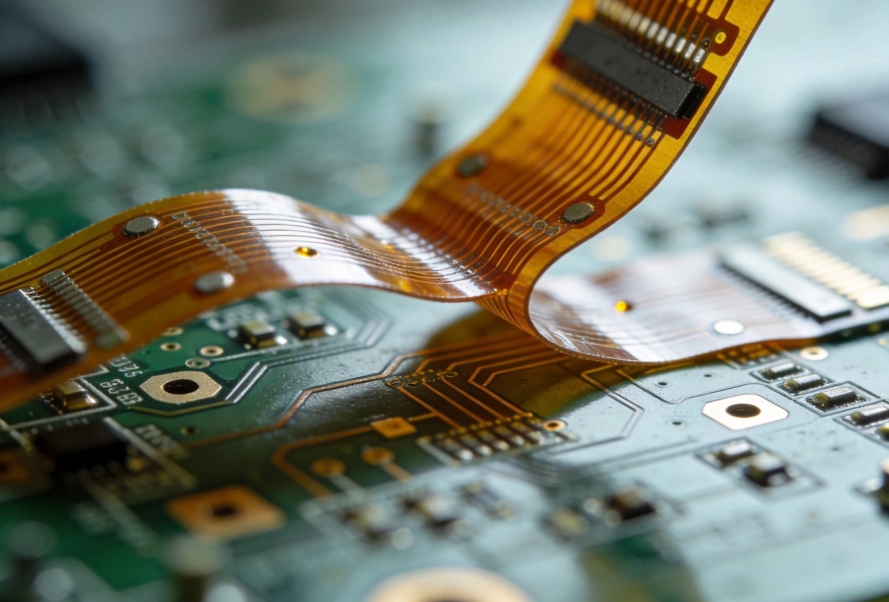
Warpage fundamentally results from differential stress within the board structure. When materials expand or contract unevenly, internal stresses develop that manifest as dimensional distortion. In thin and flexible circuits, these effects become more pronounced due to reduced material mass and increased compliance.
The most common cause of warpage involves thermal processing during Pcb Manufacturing. Multiple thermal exposures occur throughout production:
The cumulative effect of multiple thermal cycles compounds warpage. A board that appears flat after fabrication may develop measurable warpage after the first reflow, with additional warpage after subsequent assembly operations.
Flexible circuits and thin rigid boards derive mechanical properties from material laminates. When these materials are asymmetric, warpage naturally results:
Copper Distribution: Circuit traces and planes create asymmetric copper distribution across the board. Areas with more copper expand more during heating than areas with less copper. This differential expansion creates stress that bends the board toward the lighter copper side.
Stackup Asymmetry: In multi-layer boards, unbalanced construction—more copper on one side, uneven dielectric thicknesses, or asymmetric layer counts—creates inherent stress that produces warpage.
Reinforcement Asymmetry: Flexible circuits often incorporate stiffener regions for connector support or component mounting. The transition between reinforced and unreinforced areas creates stress concentrations that can propagate warpage.
Flexible circuit materials, particularly polyimide, absorb moisture from the environment. When these boards undergo thermal processing, trapped moisture rapidly vaporizes, creating internal pressure that can cause blistering, delamination, and warpage. This phenomenon, known as "popcorning," particularly affects thin boards where the mass-to-surface ratio is low.
Moisture sensitivity levels (Msl) ratings for components receive significant attention, but the board substrate itself can absorb moisture that affects processing reliability. Proper handling, storage in dry cabinets, and controlled baking before thermal exposure reduce moisture-related warpage and delamination risks.
Even after successful thermal processing, subsequent handling can introduce warpage:
Preventing warpage begins with design decisions that establish manufacturing-friendly structures. While some warpage results from process variation, design optimization significantly reduces susceptibility.
Multi-layer rigid boards should maintain structural symmetry:
Balanced Copper Coverage: Position copper on corresponding layers at similar coverage percentages. If inner layers have 40% copper coverage, balance them with outer layers at similar values. Significant imbalance creates inherent stress that warps the board.
Symmetric Layer Arrangement: Arrange layers symmetrically around the board centerline. A 4-layer stackup with 0.8mm total thickness should have equal dielectric thicknesses above and below the core centerline.
Thicker Boards for Critical Applications: When warpage tolerance is extremely tight, specify boards slightly thicker than minimum requirements. The additional material mass improves stiffness and reduces deflection from stress.
Circuit routing significantly affects warpage susceptibility:
Cross-Hatched Plane Fill: Instead of solid copper planes in thin sections, use cross-hatched patterns that provide RF shielding while allowing substrate to flex slightly without creating continuous stress lines.
Routing Geometry: Long continuous traces create directional stress. Introducing relief cuts, thermal thieving features, or breaking up large copper areas reduces Thermal Stress concentration.
Panel Utilization: Design boards to optimize panel utilization with balanced copper removal across the panel. Asymmetric panel designs create different stress distributions that manifest as non-uniform warpage.
Material properties directly influence warpage behavior:
Higher Tg Materials: Materials with higher Glass Transition Temperature (Tg) maintain dimensional stability at elevated temperatures. For lead-free processing or high-temperature applications, specify Tg170 or Tg180 materials rather than standard Tg130 FR-4.
Low-CTE Materials: Some specialized laminates incorporate ceramic fillers or other additives that reduce CTE. While more expensive, these materials significantly improve thermal stability for applications with extreme temperature cycling.
Polyimide Alternatives: For flexible circuits, polyimide offers excellent thermal stability but can be prone to moisture absorption. Consider alternative flexible materials like PET for applications where polyimide's full temperature range isn't required.
Even the best designs suffer from improper manufacturing processes. Establishing proper process controls throughout production significantly reduces warpage occurrence.
Proper storage begins before production:
Board fabrication establishes baseline flatness that subsequent processes build upon:
Vacuum Lamination: Vacuum lamination eliminates air entrapment and ensures uniform pressure distribution across the board. This reduces localized stress that leads to warpage.
Controlled Cooling: Manage cooling rates to prevent thermal shock that introduces stress. Controlled ramp-down cooling allows the board to stabilize gradually without differential temperature gradients.
Press Compensation: Experienced manufacturers profile their presses to compensate for known thermal variations. Temperature mapping of press platens identifies hot and cold spots that require adjustment.
Assembly reflow presents the greatest thermal stress challenge:
Soak Zone: Include a soak zone that gradually brings the board to reflow temperature rather than rapid heating. This reduces thermal gradients within the board that create stress.
Peak Temperature Optimization: Use the minimum peak temperature required to achieve reliable solder wetting. Excessively high peak temperatures increase stress and material degradation.
Cooling Rate Control: Controlled cooling after reflow prevents thermal shock. Nitrogen cooling or controlled convection cooling provides more uniform temperature reduction than ambient cooling.
Board Support During Reflow: For ultra-thin boards, consider reflow on aluminum carrier plates or specialized support fixtures that prevent sag and warpage during thermal exposure.
How boards are panelized and separated affects warpage:
Score-and-Break vs. Routing: V-scoring applies stress along the score line that can propagate into the board. For thin boards, routing or laser cutting creates less stress than mechanical scoring.
Tab Routing: Tab-connected panels provide support during handling and processing. Breakaway tabs should be designed to minimize stress transfer into the board during depaneling.
Depaneling Timing: Allow boards to stabilize at room temperature before depaneling. Boards removed from panels while still hot may warp as they cool.
Effective warpage management requires measurement capabilities to identify issues before they cause assembly problems:
Industry standards provide warpage Acceptance Criteria:
Ipc Standards: IPC-6012 for rigid boards and IPC-6013 for flexible circuits specify maximum warpage values based on board type and classification. Class 3 (high-reliability) boards have tighter tolerances than Class 2.
Customer Specifications: Many customers impose tighter warpage limits than Ipc Standards, particularly for fine-pitch components or specific assembly requirements. Review specifications before establishing Acceptance Criteria.
Assembly Process Capability: Ultimately, warpage limits should relate to assembly process tolerances. A board with 0.5% warpage is acceptable if your assembly process accommodates this variation.
Despite best efforts, some boards develop warpage that requires correction. Several approaches address existing warpage:
Strategic heating can redistribute stress and reduce warpage:
Heat-and-Press: Controlled heating combined with flat pressing mechanically forces the board flat while stress relaxes at elevated temperature. This requires careful temperature and pressure control to avoid damaging components or laminations.
Annealing: Gradual heating and slow cooling can relieve internal stress without mechanical force. This approach works best for warpage caused by residual stress rather than structural asymmetry.
For some warpage patterns, mechanical methods provide correction:
Vacuum Flattening: Placing warped boards under vacuum with flat surface contact gradually pulls the board flat. This works slowly but avoids thermal stress from heat-based approaches.
Weighted Cooling: For boards with minor warpage, placing weights on boards during cool storage can gradually reduce deflection. This requires extended time but introduces minimal process risk.
When warpage occurs, analyzing root causes prevents recurrence:
Flexible circuits present unique warpage challenges due to their fundamental compliance:
Warpage concerns differ based on application:
Static Flex: Flexible circuits used in bend-to-install applications should maintain flatness before installation but can tolerate some deformation during installation. Focus Warpage Prevention on the pre-installation state.
Dynamic Flex: Circuits designed for repeated flexing require attention to both installation flatness and fatigue resistance. Design stress concentration features to prevent cracks at fold lines.
Flexible circuits often incorporate stiffeners in high-stress areas:
Transition Zone Design: Gradual transitions between stiff and flexible regions reduce stress concentration that can cause delamination and warpage.
Adhesive Selection: Stiffener adhesives must maintain bond integrity through temperature cycling. Improper adhesive choice creates peel stress that warps the flexible circuit.
Coverlay (flexible soldermask) application creates asymmetric stress:
Symmetric Coverlay: When possible, apply coverlay to both sides of the flex circuit to balance stress. Single-sided coverlay inherently creates asymmetry.
Proper Cure: Coverlay requires proper cure to develop full adhesion. Under-cured coverlay can delaminate and cause warpage during subsequent processing.
Warpage in thin and flexible circuit boards results from multiple contributing factors: thermal stress during manufacturing, material asymmetry, moisture effects, and handling practices. Effective management requires addressing these factors throughout the product lifecycle, from design optimization through manufacturing process control.
Designers who understand warpage mechanisms can specify board constructions that improve manufacturability. Manufacturers who implement proper storage, handling, and process controls prevent warpage introduction during production. Quality systems that include measurement and root cause analysis continuously improve processes based on observed outcomes.
No single solution eliminates warpage entirely, particularly in ultra-thin boards where dimensional stability inherently conflicts with thickness requirements. The goal is managing warpage within limits that ensure reliable assembly and field performance. Collaboration between designers, manufacturers, and assemblers, grounded in understanding of underlying mechanisms, achieves this balance consistently.
When warpage does occur, treat it as valuable information about process capability rather than simply a defect to correct. Each warpage event offers opportunity to understand root causes and implement improvements that benefit future production.
Acceptable warpage depends on application requirements and assembly capabilities. IPC-6013 specifies maximum warpage values varying by board thickness and classification. For most applications, warpage below 0.5% is acceptable, while ultra-thin boards or fine-pitch assembly may require 0.3% or tighter. Always reference applicable IPC standards and customer specifications for specific requirements.
Correcting warpage after component assembly is challenging and risky. Heat-based correction methods can damage temperature-sensitive components. Prevention through proper handling, storage, and assembly support remains the most reliable approach. If post-assembly warpage occurs, evaluate whether it affects product function—minor warpage in non-critical applications may be tolerable.
Flexible circuits have lower bending stiffness than rigid boards, making them more susceptible to deflection from stress. Their material construction (polyimide base, adhesive layers, copper traces) creates inherent asymmetry. Additionally, flexible circuits often have thinner copper and dielectric layers that provide less resistance to deformation.
Lead-free Solder alloys require higher reflow temperatures than tin-lead solder—typically 20-30°C higher peak temperatures. These elevated temperatures increase thermal stress on the board substrate, potentially causing more warpage. Lead-free processing also requires longer soak times that can exacerbate stress effects in thin boards.
Flexible circuits should generally be stored flat with full surface support to prevent them taking a permanent set. Rolling creates bend memory that makes the circuit want to curl. If rolling is necessary for transport, use the largest practical diameter core and minimize time in the rolled condition. Ideally, receive flexible circuits in flat configurations when storage space permits.
Solving the Challenge of High-Density Interconnect (HDI) AssemblyMay/22/2026
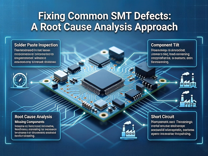
Fixing Common SMT Defects: A Root Cause Analysis ApproachJune/11/2026
The Science of Solder Paste Printing: Stencil Design Best PracticesJune/17/2026
Fiducial Marks and Tooling Holes: Ensuring Precision in SMT PlacementJuly/15/2026
Solving Assembly Stress Issues in Large and Thin PCBsSeptember/09/2026
How to Prepare Your BOM for PCB Assembly and ManufacturingOctober/15/2026
Green Manufacturing: Reducing Carbon Footprint in PCB Assembly PlantsSeptember/14/2026
Enhancing Product Lifespan with Advanced Cleaning and Coating SolutionsAugust/06/2026