Open Nav


Silkscreen markings on printed circuit boards often get treated as an afterthought—something to add after trace routing is complete. This attitude creates problems that ripple through Manufacturing, testing, and field service. When assembly technicians struggle to identify components, or when documentation references don't match board markings, the cost of poor silkscreen design becomes apparent. Bad silkscreen practices slow production, increase errors, and complicate troubleshooting. Getting silkscreen design right requires understanding how markings are applied, what information matters most, and how to balance density with readability.
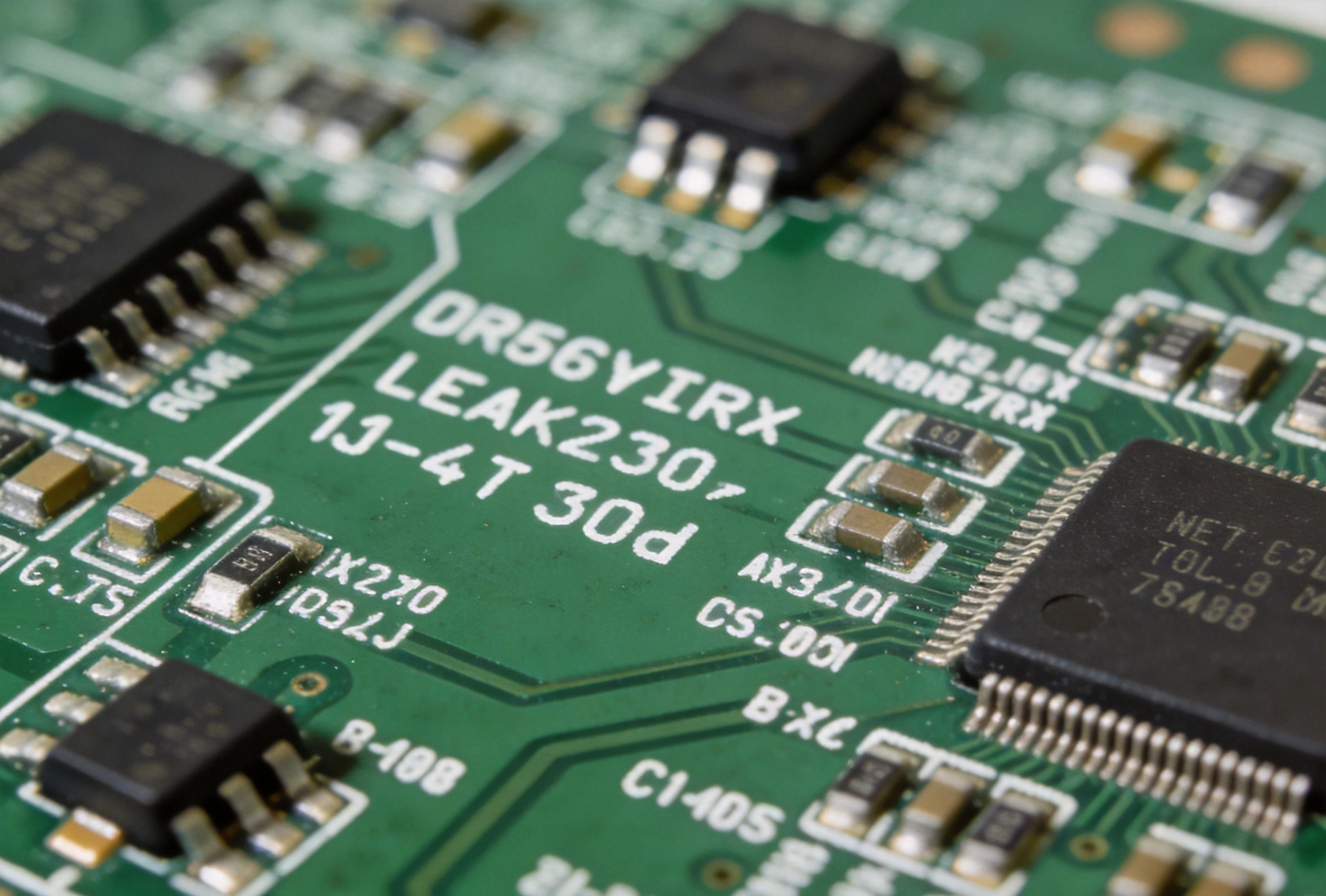
Silkscreen layers serve multiple roles in Pcb documentation. Component reference designators—R1, C3, U5—identify components for assembly, testing, and repair. Polarity markers indicate component orientation for diodes, capacitors, and ICs. Logo and revision markings communicate product identity and version. Test point labels identify locations for probe access during inspection. Together, these markings transform bare boards into documents that Manufacturing and service personnel can interpret.
The term "silkscreen" comes from the original process—pressing ink through a fine mesh screen to transfer markings onto boards. Modern PCB Fabrication uses direct legend printing, which applies markings as part of the board imaging process. Despite the technology change, the term persists. Whatever the manufacturing method, the design principles remain consistent.
Silkscreen markings must survive the board's entire lifecycle. They need to withstand handling during assembly, cleaning processes, Conformal Coating, and years of field service. Markings that fade, peel, or become illegible create problems long after initial production. Designing for durability from the start prevents these issues.
Silkscreen features have minimum manufacturable sizes. Lines narrower than the process allows either don't print or print inconsistently. Text smaller than minimum height becomes illegible, defeating the purpose of adding markings. Following industry-standard minimums ensures reliable printing without requiring special processes or cost premiums.
Standard silkscreen line width minimums typically range from 0.15mm to 0.2mm (6-8 mils) for standard production. Finer lines may be achievable but often require tighter process control and higher cost. For most applications, following standard minimums provides adequate detail without manufacturing complications.
Minimum text height depends partly on font selection and manufacturing capability. A typical minimum for readable text is 1.0mm (40 mils) for standard fonts. Smaller text may be acceptable for reference designators in dense areas, but such text should be considered supplementary to larger markings elsewhere. Legibility should never depend on magnification.
Font choice affects both manufacturing capability and readability. Simple, sans-serif fonts like Arial or Helvetica are universally available in CAD software and print reliably. Decorative fonts may look interesting but often fail to reproduce accurately through silkscreen processes. The design goal is communication, not aesthetics.
Stroke width in fonts impacts readability after printing. Very thin strokes may break during printing or wear away during board life. Bold or semi-bold weights typically provide better durability than light or thin weights. The tradeoff between style and practicality should favor practicality for production documentation.
Vector fonts (outline fonts) generally produce better results than stroke fonts in silkscreen applications. Vector fonts define character shapes explicitly, while stroke fonts reconstruct characters from line segments that may not render consistently. Converting text to outlines before generating manufacturing files ensures faithful reproduction.
Silkscreen component outlines indicate physical component boundaries. These outlines help assembly technicians verify correct component placement and orientation. Outlines also help service technicians identify component locations when replacement is needed. For some components, outlines are critical for correct orientation—integrated circuits with pin 1 indicators rely on outline visibility.
Silkscreen outlines should not overlap solder pads or other features that need clean surfaces for soldering. Solder mask typically provides the opening around pads; silkscreen should not encroach on these openings. Overlapping silkscreen onto pads creates cleaning difficulties and may affect solder joint quality.
Ipc Standards define acceptable silkscreen-to-solder-mask-clearance requirements. The typical minimum clearance from silkscreen edges to pad edges ranges from 0.1mm to 0.2mm depending on class level. Following these standards prevents manufacturing issues while maintaining adequate marking visibility.
Component marking placement should prioritize the information that assembly and test personnel need most. Reference designators should be positioned where they are visible after component placement—typically to the left or above components. Placing designators on the opposite side from placement direction means the marking becomes hidden after installation.
For surface mount components, silkscreen should be positioned to avoid interference with component body. Designators placed under component bodies serve no practical purpose since they become hidden after assembly. Positioning markers outside component footprints improves usability without requiring additional board space.
Critical polarity indicators deserve prominent placement. The cathode or anode end of electrolytic capacitors, the pin 1 corner of IC packages, and the cathode stripe on diodes should be clearly marked. These markers prevent assembly errors that could damage boards or components. When space permits, adding both silkscreen markings and physical features like beveled corners provides redundant orientation assurance.
Modern electronics designs often crowd components tightly, leaving minimal room for silkscreen markings. When component density prevents full reference designators, strategic prioritization helps. High-value components like ICs need full designators; low-value passives like decoupling capacitors often work fine with abbreviated or omitted markings if the schematic provides clear positional reference.
Silkscreen text rotation can reclaim space in tight areas. Rotating reference designators 90 degrees may allow placement in narrow channels between components. This rotation is acceptable as long as the text remains readable—excessively angled text creates interpretation difficulties.
Silkscreen density can be reduced in complex areas while maintaining full coverage elsewhere. Some designers omit silkscreen for dense passive arrays, Bga escape regions, or connector pin fields where silkscreen would create manufacturing issues. This selective approach requires judgment about which areas can safely omit markings.
Test points require clear silkscreen identification for production testing. Test point labels like TP1, TP2, or functional names like VCC, GND help test engineers locate measurement points quickly. Without clear labeling, test development takes longer and production yields suffer from misprobing.
Test point sizing matters for probe access. Test points smaller than probe tip diameters create alignment difficulties and unreliable contacts. A minimum test point diameter of 0.8mm to 1.0mm provides adequate target for standard probe tips. Larger test points improve accessibility for manual probing during debug and repair.
Via test points—using existing vias as test access points—save space but require careful design. Via test points should be connected to relevant nets, located away from component bodies, and sized appropriately for probing. Not every via makes a good test point; selecting appropriate vias for test access improves testability.
Different silkscreen ink types offer varying durability characteristics. Standard epoxy-based inks provide good durability for typical applications, surviving cleaning, handling, and extended field service. For harsh environments, specialized inks offer improved chemical resistance, temperature tolerance, or UV stability.
Ink color selection affects both appearance and durability. White silkscreen on green boards provides high contrast and good visibility. Black silkscreen on white boards offers similar contrast. Other color combinations may have reduced visibility that affects legibility, particularly under suboptimal lighting conditions.
Conformal Coating compatibility matters for boards that will receive protective coatings. Some silkscreen inks bond poorly with conformal coating materials, creating adhesion failures. Testing ink-coating compatibility prevents field failures where silkscreen delaminates from coated boards.
Assembly processes like Reflow Soldering expose silkscreen to Thermal Stress. High-temperature lead-free processes particularly challenge silkscreen adhesion. Boards that will undergo multiple high-temperature reflow cycles—common for multilayer boards with mixed technology—may experience silkscreen degradation if materials aren't specified appropriately.
Hand soldering repairs expose silkscreen to additional Thermal Stress. Soldering iron tip temperatures can exceed reflow temperatures, potentially scorching or lifting silkscreen markings. While some degradation is acceptable for internal markings, critical identifiers should be designed to withstand reasonable repair handling.
Cleaning processes affect silkscreen differently depending on chemical exposure. Aqueous cleaning, ultrasonic cleaning, and solvent cleaning each present different challenges. Specifying silkscreen inks compatible with intended cleaning processes prevents premature marking degradation.
Products with long service lives—industrial equipment, automotive systems, medical devices—need silkscreen that remains legible for years or decades. Environmental factors like UV exposure, temperature cycling, humidity, and chemical exposure all degrade silkscreen over time. Designing for extended service life means selecting appropriately durable materials.
Military and aerospace applications often specify MIL-STD requirements for silkscreen durability. These standards define test methods for evaluating marking resistance to solvents, abrasion, and environmental exposure. Following such standards ensures markings survive expected service conditions.
Product repair and refurbishment requirements should influence silkscreen durability decisions. Boards that will be repaired multiple times during product life need markings that survive repeated handling and rework. Prioritizing durability for frequently-serviced boards reduces long-term maintenance costs.
Each production board should carry identification markings beyond component references. Board part number, revision level, date code, and manufacturing source identification enable traceability throughout production and service life. These markings transform boards from anonymous assemblies into documented products.
Revision level markings communicate design evolution. Rev A, Rev B, Rev C designations allow production and service personnel to verify board versions. Mismatched revisions between documentation and physical boards create confusion and potential errors. Clear revision marking prevents these issues.
Date codes enable manufacturing lot traceability. When quality issues emerge, date codes allow targeting affected production runs for containment actions. Without date code marking, recall scope must expand to cover all potentially affected units rather than specific lots.
Silkscreen must align with schematic and Assembly Documentation. Reference designators on boards should exactly match those in schematics and Bills of Materials. Discrepancies between silkscreen and documentation create errors when technicians follow documents that don't match physical boards.
Assembly drawings that supplement silkscreen markings should reference board markings clearly. If assembly drawings indicate special instructions for certain components, corresponding silkscreen reference simplifies verification. Silkscreen and documentation should work together as an integrated information system.
Silkscreen legibility verification should be part of first-article inspection. Checking that silkscreen prints correctly, marks are legible, and documentation matches board markings catches problems before production scales up. This verification is especially important for new designs or after design changes.
Trying to include too much information in silkscreen creates readability problems. When component density prevents clear silkscreen placement, selective marking serves better than cluttered marking. Prioritizing essential information and omitting nice-to-have details improves overall clarity.
Silkscreen that overlaps itself or other features indicates planning problems. Crossing text lines, obscured markings, and illegible characters suggest that silkscreen design wasn't considered until routing was complete. Treating silkscreen as an integral part of layout planning prevents these issues.
Silkscreen too close to pads creates solderability problems. When silkscreen ink overlaps pad areas, cleaning becomes difficult and solder joints may be compromised. Maintaining specified clearances from silkscreen to pad edges ensures reliable soldering.
Insufficient spacing between silkscreen characters affects readability. Crowded text becomes difficult to distinguish, particularly for similar-looking characters like O and 0, or l and 1. Adequate character spacing improves readability without requiring additional board area.
Polarity markings that don't match component orientation defeat their purpose. When IC pin 1 indicators are placed incorrectly, assembly technicians may install components backwards. Precise alignment of silkscreen polarity markers with actual component orientation prevents assembly errors.
Silkscreen rotation that doesn't match component rotation creates similar problems. If silkscreen text is oriented for viewing from one direction but components are placed for viewing from another, confusion results. Consistent orientation conventions eliminate this problem.
Ipc Standards define silkscreen requirements for different reliability classes. IPC Class 1 (general electronic products), Class 2 (dedicated service electronics), and Class 3 (high-reliability electronics) each have different marking requirements. Understanding which class applies to your product ensures appropriate silkscreen specification.
Ipc-a-610 covers silkscreen acceptability criteria for assembled boards. While this standard focuses on assembled boards rather than bare boards, its criteria for component identification and marking legibility provide useful guidance for silkscreen design.
Design for Manufacturability (DFM) reviews should include silkscreen assessment. Whether conducted internally or by your manufacturing partner, DFM reviews catch silkscreen issues before they cause production problems. Early identification of silkscreen concerns reduces cost and schedule impact compared to late discovery.
Some customers impose additional silkscreen requirements beyond standard IPC criteria. Automotive customers often require specific marking formats, traceability information, and durability qualifications. Medical device requirements may specify particular fonts, minimum text heights, or marking permanence standards.
Export compliance marking requirements may apply to certain products. CE marking, FCC identification, and country-of-origin markings have specific placement and format requirements. Understanding which compliance markings apply to your product ensures necessary markings are included.
Treating silkscreen as an afterthought leads to problems. Integrating silkscreen considerations from the beginning of layout planning ensures adequate space for necessary markings. Component placement decisions should account for silkscreen placement needs.
Silkscreen requirements should be documented in design standards or guidelines. When multiple designers work on related products, consistent silkscreen practices improve manufacturing and service efficiency. Design guidelines codify best practices for reuse across projects.
Silkscreen verification should be part of design review checklists. Checking silkscreen placement, text legibility, and documentation alignment during design review catches issues before files go to manufacturing. Formal review gates prevent silkscreen problems from reaching production.
Manufacturing capability varies for silkscreen features. Before finalizing silkscreen design, confirming capabilities with your fabrication partner prevents surprises. Some manufacturers handle fine-line silkscreen readily; others prefer standard specifications. Matching design to capability improves first-pass success.
Design rule files should include silkscreen specifications. When design rules define silkscreen minimums, spacing, and clearance requirements, violations are caught during design rather than during manufacturing. This proactive approach reduces iteration cycles and improves time to production.
Silkscreen proofing options may be available from fabrication partners. Reviewing silkscreen artwork before production allows corrections without manufacturing impact. This proofing step is particularly valuable for complex boards with extensive silkscreen requirements.
Minimum silkscreen text height typically ranges from 0.8mm to 1.0mm depending on manufacturer capabilities and IPC class requirements. Some manufacturers can produce smaller text, but standard production usually works reliably with 1.0mm minimum height. Always verify capabilities with your specific fabrication partner before designing small text.
Silkscreen over vias is generally not recommended. Vias create uneven surfaces that affect ink application and coverage. Exposed vias under silkscreen may allow ink to enter barrel holes, creating aesthetic or functional issues. Keep silkscreen clear of vias unless the manufacturer specifically supports via-in-marking processes.
Essential silkscreen for assembly includes component reference designators, polarity indicators for diodes and capacitors, pin 1 markers for IC packages, and test point labels. Additional markings for board identification, revision level, and traceability support manufacturing and service processes. The extent of marking depends on product complexity and service requirements.
Silkscreen removal from finished boards requires careful chemical or mechanical processes. Solvent-based removal can damage underlying surfaces if not done carefully. Laser ablation offers precision removal without chemical concerns. In most cases, it is easier to avoid silkscreen errors during design rather than correct them after board fabrication.
Basic silkscreen marking is typically included in standard Pcb pricing. Special silkscreen requirements—finer lines, non-standard colors, extended durability specifications—may add cost. Multiple silkscreen layers or selective silkscreen marking also affect pricing. Standard silkscreen practices keep costs predictable.
Silkscreen design deserves attention as an integral part of PCB development, not as a final checkbox item. Well-designed silkscreen supports manufacturing efficiency, enables effective testing, and aids field service throughout product life. Poor silkscreen design creates hidden costs that accumulate throughout production and service.
The principles covered here—appropriate sizing, strategic placement, durability planning, and documentation alignment—apply across different product types and reliability requirements. Adapting these practices to specific applications and industry requirements helps ensure silkscreen investments pay dividends.
Investing time in silkscreen planning during design prevents manufacturing and service problems later. When silkscreen is done right, boards communicate clearly to everyone who handles them, from initial assembly through final service. This clarity reduces errors, improves efficiency, and ultimately delivers better products to end users.

Thermal Relief Design: Balancing Heat Dissipation and SolderabilityJuly/23/2026

Optimizing Pad Design to Prevent Tombstoning and BridgingJune/05/2026

Mastering DFM: Essential Design Rules for Flawless PCB AssemblyMay/22/2026

China's Role in the Global PCB Assembly Ecosystem: A 2026 UpdateAugust/11/2026

Fiducial Marks and Tooling Holes: Ensuring Precision in SMT PlacementJuly/15/2026

Managing Moisture Sensitivity Levels (MSL) for BGA and QFN PackagesAugust/10/2026

The Science of Solder Paste Printing: Stencil Design Best PracticesJune/17/2026

Designing for Testability (DFT): Placing Test Points for ICT and FCTJuly/31/2026