

The moment you pick up a heavy copper Pcb for the first time, you know this is not your standard FR-4 board. These are thick, weighty circuit boards designed to handle serious current, survive harsh environments, and keep industrial equipment running without interruption. But that same robustness that makes heavy copper PCBs valuable is what makes them notoriously difficult to assemble. Standard reflow profiles fall short, component placement demands specialized fixtures, and solder joints behave differently when you are dealing with copper weights of 3 oz or more per square foot.
If you have run into these challenges, you are not alone. Engineers and manufacturers across automotive, aerospace, energy, and industrial controls sectors face the same struggles when working with thick copper designs. This guide walks through practical solutions that experienced manufacturers use to successfully assemble heavy copper PCBs without sacrificing reliability or throughput.
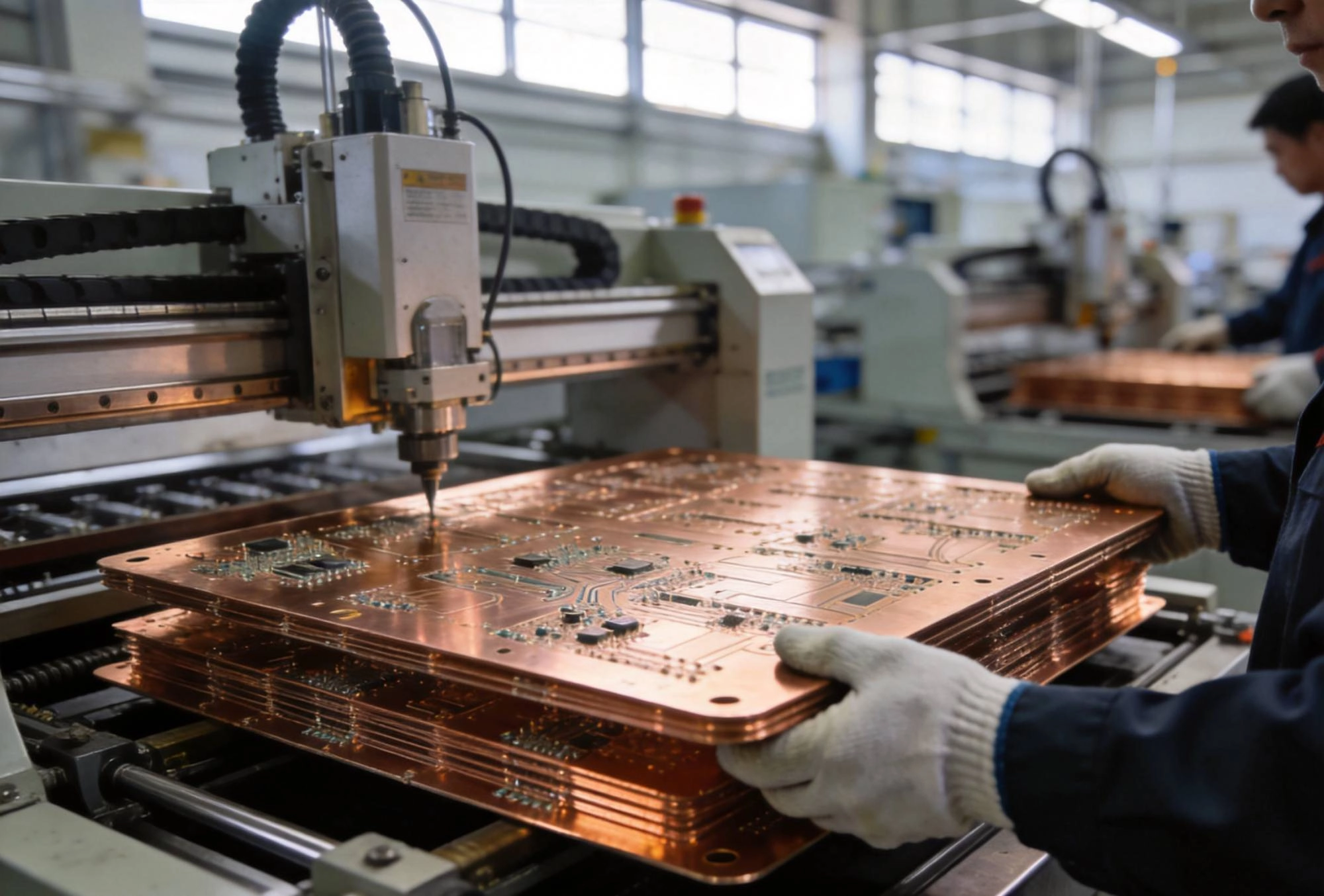
Before diving into solutions, it helps to understand what makes heavy copper PCBs fundamentally different during assembly. Standard Pcb copper thickness is typically 1 oz per square foot, which translates to about 35 micrometers. Heavy copper designs start at 2 oz and go up to 20 oz or even higher in extreme cases. That difference in copper mass changes everything about thermal dynamics during soldering.
When you run a standard reflow profile on a heavy copper board, the thermal mass of the thick copper acts like a heat sink. The焊膏 paste melts, but the copper traces and planes absorb that heat energy faster than the solder can reflow properly. The result is incomplete wetting, cold joints, or in some cases, components that shift during reflow because the surrounding copper planes are pulling heat away unevenly.
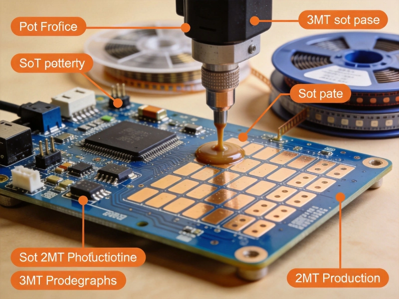
Heavy copper PCBs also present mechanical challenges. The boards are heavier and stiffer, which affects pick-and-place accuracy and can stress component leads during handling. Plane structures are more prominent, creating uneven surfaces that complicate stencil alignment and Solder Paste Deposition.
The most critical adjustment for heavy copper assembly is your reflow profile. Standard SAC305 solder profiles typically feature a ramp rate of 1-3°C per second and a peak temperature around 245-260°C. For heavy copper boards, you need to account for the additional thermal load by increasing soak time in the pre-heat zone and raising peak temperatures slightly.
A well-tuned profile for a 4 oz copper board might look like this: start with a longer pre-heat soak between 150-180°C to bring the entire board temperature equilibrium slowly. Extend the time above liquidus to give solder joints adequate time to form properly. Increase peak temperature by 5-10°C and consider longer cooling ramps to reduce thermal shock. Many manufacturers find that nitrogen atmosphere reflow helps significantly with heavy copper assemblies because it reduces oxidation and improves wetting behavior on the thick copper surfaces.
Heavy copper boards often benefit from HASL (Hot Air Solder Leveling) with longer dwell times or ENIG (Electroless Nickel Immersion Gold) finish. HASL provides a solderable surface that is more forgiving during assembly, while ENIG offers excellent flatness for fine-pitch components and consistent solderability even on thick copper plane structures. The choice between these depends on your component mix, board flatness requirements, and operating environment.
For the most challenging heavy copper assemblies, vapor phase soldering has emerged as a proven solution. In vapor phase reflow, the board is heated by condensation of a specialized fluid vapor, which transfers heat very efficiently and uniformly regardless of copper weight variations. This method eliminates the hot spots and uneven heating that plague forced-air reflow ovens when dealing with thick copper thermal mass.
Heavy copper boards require more robust support during component placement. Standard PCB carriers may not provide adequate support for the increased weight, leading to placement errors or board flex that damages components. Invest in custom fixturing that supports the board fully and provides consistent reference points for your pick-and-place system.
Vacuum pick-up nozzles work better than mechanical grippers for placing components on heavy copper boards because the uneven topography caused by thick plane structures can interfere with mechanical gripping mechanisms. If you are using Bga or Qfn packages, consider using vision systems with multiple fiducial points to compensate for any slight distortions in the board surface.
Heavy copper boards with asymmetric copper distribution can experience warpage during reflow. This is especially problematic when one side of the board has significantly more copper than the other. Solutions include using symmetric layer stack-ups, adding copper thieving patterns to balance thermal mass, and implementing a cool-down profile that reduces thermal gradients across the board.
For boards that remain prone to warpage, consider using a hot belt puller or controlled cool-down chamber after reflow to maintain flatness while the solder solidifies.
Heavy copper PCBs frequently use heavy copper vias designed to handle high current flow between layers. These vias often require solder fill to ensure reliable interconnections, especially when the board will see thermal cycling in industrial environments. Standard Wave Soldering may not adequately fill these vias, so consider selective solder fill processes or manual solder pot dipping for critical vias.
Hole fill testing according to Ipc Standards is essential for heavy copper boards. Not all plating processes create vias that can be reliably filled, so work with your fabricator to specify appropriate hole preparation and verify fill rates on prototype boards before committing to production.
For very high current applications, some designs use press-fit terminals or bolted connections rather than relying solely on solder joints. Press-fit technology provides a gas-tight connection through mechanical interference between the terminal and plated through-hole. This approach eliminates solder joint reliability concerns for high-current connections and simplifies field serviceability.
When using press-fit connectors on heavy copper boards, ensure that the board thickness and hole sizing accommodate the press-fit requirements. Heavy copper boards may need modified hole sizes or specialized press-fit zones to achieve proper connection without damaging the board or connector.
Heavy copper assemblies demand more rigorous inspection than standard boards. Bga packages, QFNs, and any components under which solder joints are hidden require X-ray inspection to verify joint integrity. The thick copper planes can obscure solder joints in standard X-ray systems, so ensure your inspection equipment has sufficient resolution and penetration for heavy copper applications.
Cross-section analysis of prototype boards provides valuable data for setting Acceptance Criteria. Understanding how solder wets on your specific copper weight and finish combination helps establish realistic inspection standards.
Industrial applications often expose PCBs to thermal cycling, vibration, and humidity. Heavy copper boards can actually perform better in these environments because the thick copper provides superior thermal conductivity and current handling, but only if the solder joints are properly formed. Always validate your assembly process with thermal cycling tests that simulate your target operating environment.
Many manufacturers skip vibration testing on heavy copper assemblies assuming the thick boards are inherently rigid, but this assumption can lead to field failures. Heavy copper boards with poor solder joints can crack under vibration even though the board substrate remains intact.
Successfully assembling heavy copper PCBs requires close collaboration between the designer, fabricator, and assembler. Make sure all parties understand the copper weight, expected current flow, and operating environment. Provide your CM with thermal simulation data if available, and request process capability studies on prototype runs before committing to production volumes.
Ask your CM about their experience with heavy copper assemblies specifically. General pcb assembly expertise does not automatically translate to heavy copper competency. Find out what reflow equipment they use, whether they have vapor phase capability, and how they handle warpage management.
Working with your designer to optimize the board for assembly can significantly improve outcomes. Consider adding thermal relief patterns around pads to reduce heat sinking during hand repairs. Specify keep-out areas around large plane structures to give assembly equipment access. Balance copper distribution across layers to minimize warpage potential. These small adjustments cost little in design time but can prevent significant Manufacturing headaches.
One of the most common mistakes is assuming that heavy copper boards can use the same assembly processes as standard PCBs with just minor tweaks. While profile adjustments help, truly reliable heavy copper assembly often requires dedicated equipment or significant process development. Another pitfall is under-specifying copper weight. If your fabricator builds a board with lighter copper than specified, your assembly processes will be over-engineered for the actual product and may cause other problems.
Finally, do not neglect the consequences of mixing standard components with heavy copper constructions. Component datasheets specify thermal tolerances that assume the component is mounted on a standard PCB. If your board has significantly different thermal characteristics, you may need to de-rate components or select parts with higher thermal ratings.
Assembling heavy copper PCBs for industrial applications presents real challenges, but these challenges are solvable with the right approach. Success starts with understanding how thick copper changes thermal dynamics during assembly and adjusting your reflow profiles accordingly. From there, investing in proper fixturing, choosing appropriate finishing processes, and implementing rigorous inspection protocols will get you to reliable production.
The extra effort required for heavy copper assembly pays off in the final product. Heavy copper PCBs deliver superior current handling, better Thermal Management, and improved reliability in demanding industrial environments. Working with experienced partners who understand both PCB Fabrication and heavy copper assembly processes makes the difference between a successful product launch and a costly set of Manufacturing surprises.
Boards with 2 oz copper per square foot or heavier typically benefit from modified reflow profiles and enhanced inspection. While some standard processes can accommodate 2 oz copper, anything at 3 oz or above almost always requires dedicated process adjustments. The exact threshold depends on board size, layer count, and component density.
Yes, with modifications. Standard pick-and-place equipment can handle heavy copper boards, but you may need enhanced board support fixturing, adjusted pick-up nozzle sizes, and modified vision systems to account for uneven board surfaces. Reflow oven profiles need significant adjustment for anything above 2 oz copper.
Preventing warpage starts at the design stage with symmetric layer stack-ups and balanced copper distribution. During assembly, use slower ramp rates, extended soak times, and controlled cooling profiles. For particularly sensitive boards, consider vapor phase reflow or hot belt pullers during cool-down to maintain flatness.
Visual Inspection, X-ray inspection for hidden joints, and cross-section analysis for prototype validation are essential. For production boards, AOI (Automated Optical Inspection) may have limited effectiveness on heavy copper boards due to surface topography, so X-ray inspection becomes more important for verifying BGA and Qfn solder joints.
ENIG is generally preferred for fine-pitch components and boards requiring flat surfaces, while HASL works well for through-hole dominant designs and applications where hand rework might be needed. For high-current applications, both finishes work adequately, but ENIG provides more consistent solderability across varied copper thicknesses within the same board.
Need help with your heavy copper pcb assembly project? Our engineering team has extensive experience with thick copper designs for industrial applications. Contact us to discuss your specific requirements and manufacturing challenges.

Cost-Reduction Strategies Without Compromising PCBA QualityJuly/09/2026

Overcoming Supply Chain Shortages: Alternative Component Sourcing StrategiesMay/22/2026
Solving the Challenge of High-Density Interconnect (HDI) AssemblyMay/22/2026

Fixing Common SMT Defects: A Root Cause Analysis ApproachJune/11/2026
Bridging the Gap Between R&D Prototypes and Stable Mass ProductionJuly/27/2026
Downloadable Resources: DFM Checklists and BOM TemplatesAugust/03/2026
What is PCB Assembly? A Beginner's Guide to the BasicsMay/22/2026
Fiducial Marks and Tooling Holes: Ensuring Precision in SMT PlacementJuly/15/2026